Solder mask zero-clearance PCB preparation method

A PCB board and solder mask technology, applied in the field of PCB board preparation with zero clearance for solder mask, can solve the problems of solder mask bridge falling off, excessive undercut, electrical performance failure, etc., to ensure completeness, avoid excessive undercut, The effect of reducing the difficulty of the process

Inactive Publication Date: 2020-03-27
广州广合科技股份有限公司
View PDF5 Cites 2 Cited by
  • Summary
  • Abstract
  • Description
  • Claims
  • Application Information

AI Technical Summary

Problems solved by technology

At the same time, the development process is also likely to cause the problem of excessive undercut, and the resulting problem of solder mask bridge falling off, resulting in electrical performance failure

Method used


Image

  • Solder mask zero-clearance PCB preparation method
  • Solder mask zero-clearance PCB preparation method
  • Solder mask zero-clearance PCB preparation method

Examples


Embodiment Construction

[0035] Such as Figure 1-4 As shown in, a method for preparing a PCB board with solder resistance and zero clearance provided by an embodiment of the present invention includes the following steps:

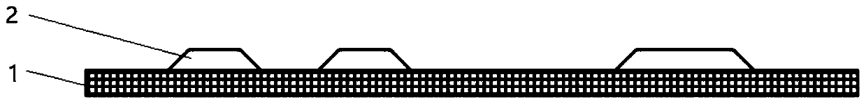
[0036] S1, feeding, place the base material 1 on the processing station, and fix it (such as figure 1 shown);

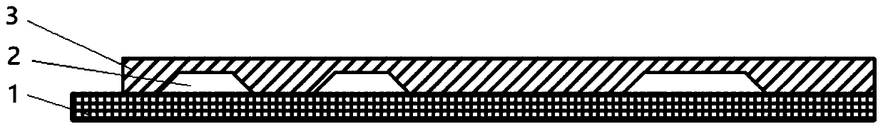
[0037] S2. For the first screen printing, the screen printing process of stretching, degreasing, pre-drying, exposure, development, and drying is carried out in sequence. In the exposure process, selective exposure is used to reserve the window area of ​​the substrate 1 to complete the first screen printing. get semi-finished products (such as figure 2 shown);

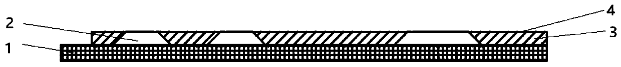
[0038] S3, grind the plate, adopt the process of mechanical brushing to carry out template processing to the semi-finished product, remove the ink layer 3 on the surface of the circuit 2 and the surface of the pad 4, and keep the ink layer 3 between the lines 2 (such as image 3 shown);

[0039] S4, cleanin...


PUM


Abstract

The invention relates to a solder mask zero-clearance PCB preparation method, which comprises the following steps of: feeding: a base material is placed at a processing station and fixing the base material; first screen printing: the screen printing process of stretching, degreasing, pre-drying, exposing, developing and drying is conducted in sequence, in the exposing process, selective exposingis adopted for reserving the windowing area of the base material, and screen printing for the first time is completed to obtain a semi-finished product; board grinding: the template treatment is carried out on the semi-finished product by adopting a mechanical grinding and brushing process, the ink layers on the surfaces of the circuits and the surfaces of the bonding pads are removed, and the inklayers between the circuits are reserved; the impurities on the plate surface are cleaned and removed; screen printing is conducted for the second time, the screen printing process of stretching, degreasing, pre-drying, exposing, developing and drying is conducted again, and the area needing to be shielded is covered with the ink layer again; and a finished product with zero clearance is obtained. The problems of solder mask exposure deviation and solder mask upper PAD are avoided; the problems of overlarge undercut and solder mask bridge falling caused by development are avoided, the factorsinfluencing the circuit are reduced, and the process difficulty is reduced.

Description

technical field [0001] The invention relates to the field of circuit board preparation, in particular to a method for preparing a PCB board with solder resistance and zero clearance. Background technique [0002] The solder mask is composed of a cured ink layer, which is of great significance to the PCB board. It can prevent the circuit short circuit caused by the overflow of the solder. At the same time, it can prevent the non-soldering points from being contaminated by the solder during wave soldering, and it can also play a moisture-proof effect. protect the circuit. [0003] However, due to the increasing integration of PCB circuits today, the reliability of the solder bridge (the ink layer between the embedded circuits on the PCB board) is also facing higher challenges. The conventional process of assembly welding preparation is to cure the ink layer at the designated position by means of exposure and opening, and then wash off the ink layer at the excess position thro...

Claims


Application Information

Patent Timeline
Patent Type & Authority Applications(China)
IPC IPC(8): H05K3/28
CPCH05K3/282H05K2203/025H05K2203/052
Inventor 倪浩然兰富民章宏郑剑坤
Owner 广州广合科技股份有限公司
Why Eureka
Try Eureka