Two-dimensional mosfet/mfis multifunctional switching memory device and its preparation method

A multi-functional switch and storage device technology, which is applied in semiconductor/solid-state device manufacturing, static memory, digital memory information, etc., can solve the problems that hinder the wide use of FRAM, the ferroelectric thin film is not expandable, and the ferroelectric performance is weakened, so as to achieve the function Rich, highly integrated, low-cost effects

Active Publication Date: 2021-02-09
ZHEJIANG XINKE SEMICON CO LTD
View PDF6 Cites 0 Cited by
  • Summary
  • Abstract
  • Description
  • Claims
  • Application Information

AI Technical Summary

Problems solved by technology

There are many limitations in the ferroelectric material in the classical FRAM structure. This is because the traditional ferroelectric film is not scalable, and when its thickness is reduced, the ferroelectric performance weakens or even disappears. As a result, FRAM has not broken through the 130 nanometer technology node, which hinders the traditional Widespread use of FRAM

Method used


Image

  • Two-dimensional mosfet/mfis multifunctional switching memory device and its preparation method
  • Two-dimensional mosfet/mfis multifunctional switching memory device and its preparation method
  • Two-dimensional mosfet/mfis multifunctional switching memory device and its preparation method

Examples


Embodiment Construction

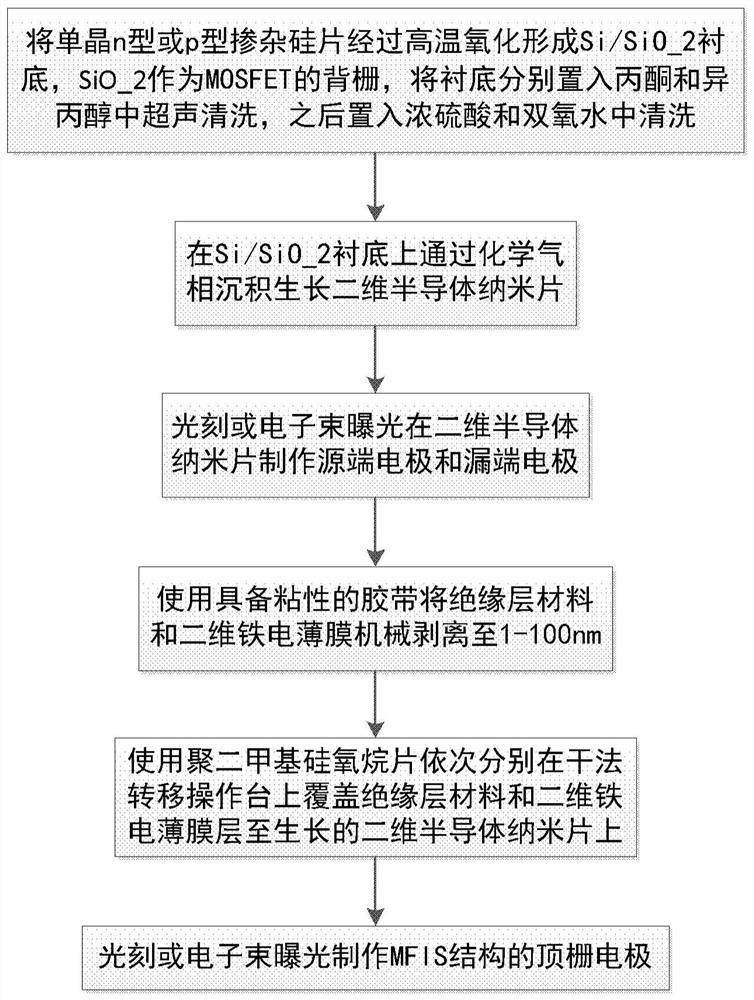
[0044] In order to make the purpose, technical solutions and advantages of the present invention clearer, the present invention will be described in further detail below in conjunction with specific embodiments and with reference to the accompanying drawings, but the following embodiments are only illustrative, and the protection scope of the present invention does not Not limited by these examples.

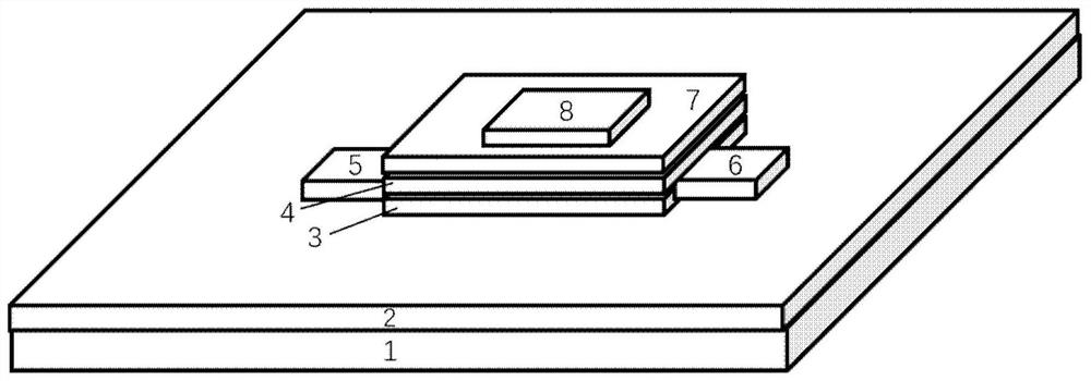
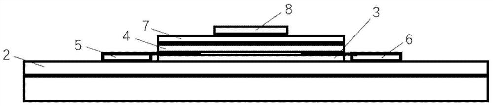
[0045] see figure 1 and figure 2 , an embodiment of the present invention provides a two-dimensional MOSFET / MFIS multifunctional switch storage device, including:

[0046] p-type or n-type doped Si bottom gate electrode 1;

[0047] A silicon dioxide gate dielectric 2 is disposed on the bottom gate electrode 1;

[0048] The two-dimensional semiconductor nanosheet 3 serves as a channel and is disposed on the silicon dioxide gate dielectric 2;

[0049] Cubic boron nitride insulating layer 4, the edge of which is aligned with the two-dimensional semiconductor nanosheet 3 and arr...


PUM

PropertyMeasurementUnit
thicknessaaaaaaaaaa
thicknessaaaaaaaaaa
thicknessaaaaaaaaaa

Abstract

The invention discloses a two-dimensional MOSFET / MFIS multifunctional switch storage device and a preparation method thereof, and prepares a nanoscale multifunctional device with a comprehensive two-dimensional structure integrating switch and storage characteristics. Among them, the MOSFET structure is doped Si, silicon dioxide, two-dimensional semiconductor nanosheets and source-drain electrodes to realize the switching function; the MFIS structure includes top gate electrodes, two-dimensional ferroelectric films, cubic boron nitride insulating layer sheets, two-dimensional thin A layer of semiconductor nanosheets and source and drain electrodes to realize the storage function. The field effect transistor with two-dimensional material as the channel has a mobility of 700cm2 / Vs, and the on-off ratio exceeds 108; the two-dimensional ferroelectric film is used as a ferroelectric material to replace the traditional MFIS, breaking through the thickness limit of the ferroelectric film, making its thickness Reduced to the thickness of a single atomic layer, about 1nm, the polarization direction of the ferroelectric film can be changed by the voltage applied to the top gate to realize non-volatile information storage. The unique two-dimensional MOSFET / MFIS structure greatly improves transistor integration and information storage density.

Description

technical field [0001] The invention relates to the fields of semiconductor field effect transistors and non-volatile information storage, in particular to a design and preparation method of a new type of MOSFET / MFIS multifunctional switching storage device based on two-dimensional ferroelectric materials. The invention firstly realizes a multi-functional unit device with a nano-scale process integrating switch and storage characteristics with a comprehensive two-dimensional structure. Background technique [0002] According to "Moore's Law", every 18 months, the number of transistors that can be accommodated on an integrated circuit will double, and the performance will also double. However, traditional silicon-based transistors will soon reach their physical limits due to the constraints of quantum effects. Therefore, looking for semiconductor transistor materials to replace silicon-based semiconductors is currently a hot topic in the field of semiconductor research world...

Claims


Application Information

Patent Timeline
Patent Type & Authority Patents(China)
IPC IPC(8): H01L29/78H01L21/34G11C11/22
CPCG11C11/223G11C11/225H01L29/66969H01L29/78391
Inventor 魏钟鸣杨淮李京波
Owner ZHEJIANG XINKE SEMICON CO LTD
Why Eureka
Try Eureka