

Heterogeneous material structured multilayer film wave absorber and manufacturing method thereof
A technology of multi-layer thin films and heterogeneous materials, applied in metal material coating process, coating, gaseous chemical plating, etc., can solve the problems of large volume and weight of the absorber, narrow bandwidth of the absorber, and high manufacturing cost , to achieve the effects of high manufacturing efficiency, low manufacturing process cost, and reduced volume and weight
- Summary
- Abstract
- Description
- Claims
- Application Information
AI Technical Summary
Problems solved by technology
Method used
Image

Examples
Embodiment 1
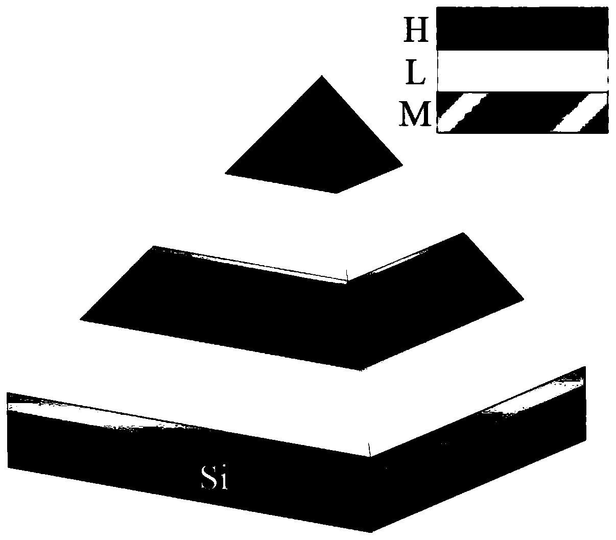
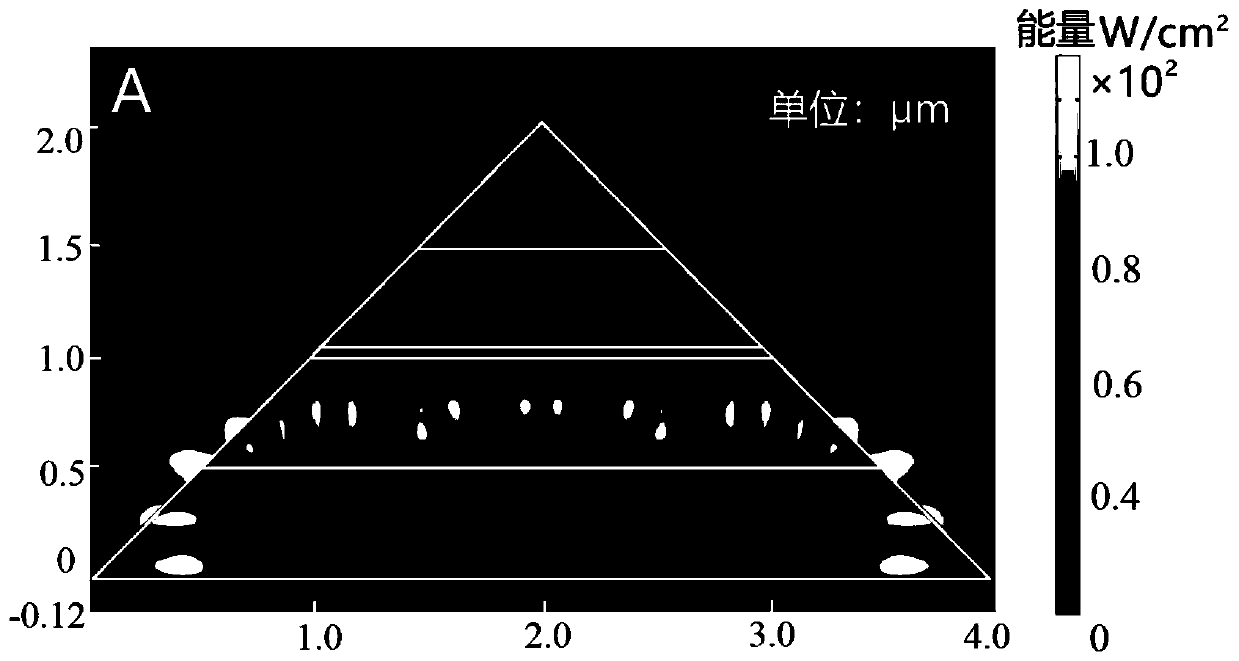
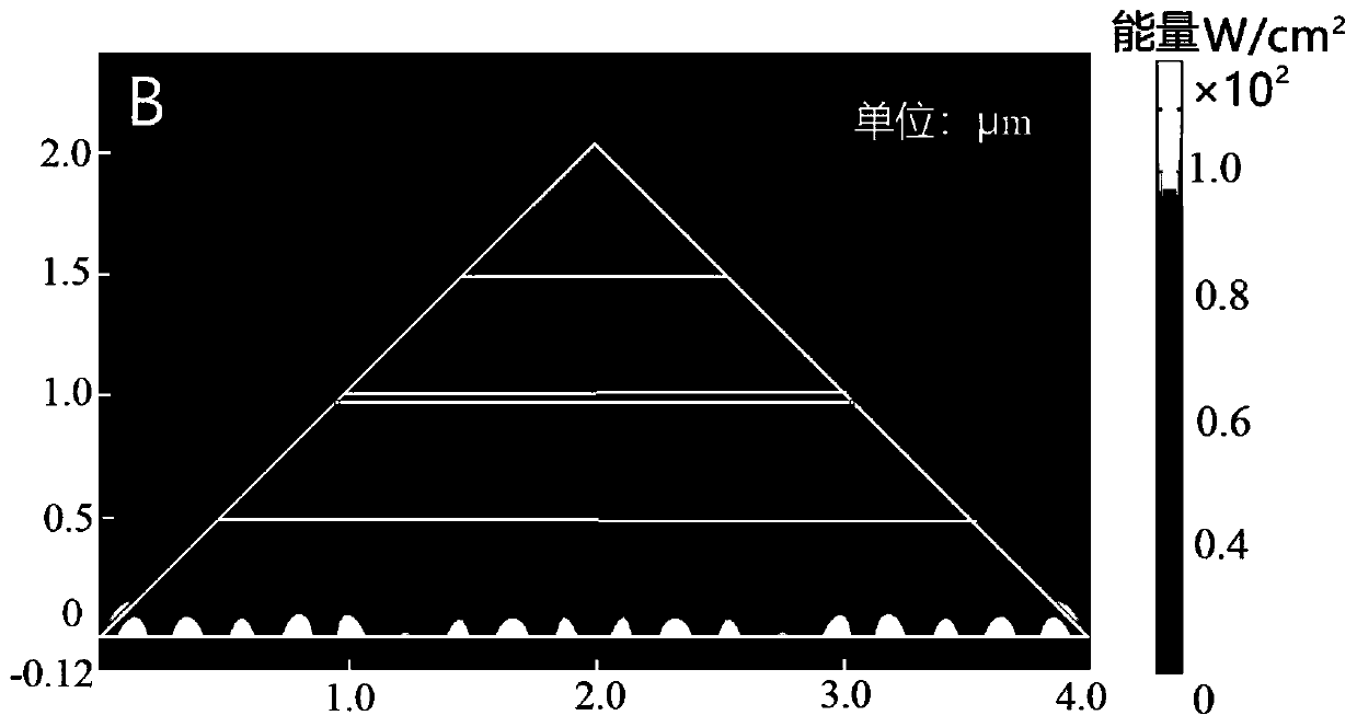
[0025] Such as figure 1 As shown, the present invention provides a heterogeneous material structured multi-layer thin film absorber. This embodiment is a six-layer thin film absorber, including a silicon substrate, and two multi-film layer units are arranged on the top of the silicon substrate, namely metal -Low refractive index layer-high refractive index layer (M-L-H), each multi-film layer unit includes Ag thin film, SiO 2 Thin films and SiN x Thin film, two multi-film layer units as a whole pyramid array structure. The size of the silicon substrate is 4 μm×4 μm, and the height of the pyramid array structure composed of two multi-layer units is 2 μm. The film thickness of each multi-film layer unit is set as follows: figure 1 As shown, the Ag film thickness in the film layer unit is 40nm, and the SiO 2 The thickness of the film is 490nm, SiN x The thickness of the film was 490 nm. Since the thickness of the Ag film on the surface of the substrate is not less than 120n...
Embodiment 2
[0034] Same as Example 1, the absorbing structure of each "metal-low refractive index layer-high refractive index layer (M-L-H)" is designed as a multi-film layer unit. In this embodiment, three multi-film layers are arranged on the top of the silicon substrate Layer unit, the three multi-film layer units are a pyramid array structure as a whole. The size of the silicon substrate is 4 μm×4 μm, and the height of the pyramid array structure composed of three multi-layer units is 1.8 μm. The film thickness of each film unit is set as follows: Ag film thickness is 200nm, SiO 2 The thickness of the film is 200nm, SiN x The thickness of the film is 200nm, as Figure 4 shown.
[0035] The preparation method of said nine-layer film wave absorber comprises the following steps:
[0036] 1. Using magnetron sputtering technology to deposit a metal thin film on the surface of the silicon substrate, and by controlling the deposition time, the thickness of the Ag film is 200nm.
[0037]...
PUM
| Property | Measurement | Unit |
|---|---|---|
| Thickness | aaaaa | aaaaa |
| Thickness | aaaaa | aaaaa |
| Thickness | aaaaa | aaaaa |
Abstract
Description
Claims
Application Information