Superlattice memristor functional layer material, memristor unit and manufacturing method thereof

A memristor and functional layer technology, applied in the field of superlattice memristor and its preparation, can solve the problem of limiting the storage capacity of memristor memory chips, restricting the research of peripheral circuits of artificial neural network chips, and poor linearity of synapse characteristics To achieve the effect of improving stability and consistency, continuously adjusting synaptic characteristics, and improving synaptic linearity

Active Publication Date: 2020-04-14
HUAZHONG UNIV OF SCI & TECH
View PDF7 Cites 8 Cited by
  • Summary
  • Abstract
  • Description
  • Claims
  • Application Information

AI Technical Summary

Problems solved by technology

This severely limits the storage capacity of memristor memory chips, and also poses great challenges to the large-scale integration and circuit design of memristors.
On the other hand, in the field of modern brain-inspired neuromorphic computing, memristors, as synaptic element conductive filaments, will lead to a sudden increase in the conductance of the device at the moment of formation of the dielectric layer, which is not in line with the expected conductance of memristors in brain-inspired simulations. The requirement of continuously changing with the external electric field, the linearity of the synaptic characteristics is generally poor, which also seriously restricts the research on the peripheral circuits of the artificial neural network chip, which not only increases the design cost, but also increases the circuit area

Method used


Image

  • Superlattice memristor functional layer material, memristor unit and manufacturing method thereof
  • Superlattice memristor functional layer material, memristor unit and manufacturing method thereof
  • Superlattice memristor functional layer material, memristor unit and manufacturing method thereof

Examples


preparation example Construction

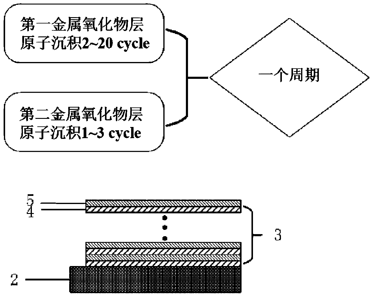
[0061] Specifically, in the above-mentioned memristor unit, applying a specific external excitation / SET operation is used to set a logic 1, and when an opposite external excitation is applied, the / RESET operation is a logic 0. By applying a certain logic circuit to the above-mentioned memristor unit, controlling the on-off of the oxygen vacancy conductive filament can realize the storage of logic sequence and data. In the present invention, a method for preparing the above-mentioned superlattice memristor is also provided, comprising the following steps:

[0062] Step 1: preparing the first electrode 2 on the substrate 1 by physical vapor deposition;

[0063] Step 2: A superlattice memristor functional layer 3 is prepared on the first electrode 2 in step 1 by atomic layer deposition; wherein, firstly, a layer of 2 to 15 atomic layers is prepared on the first electrode 2. The first metal oxide layer 4, and then prepare a second metal oxide layer 5 of 1 to 3 atomic layers on ...

Embodiment

[0070]The invention is further explained below with reference to the schematic examples shown in the accompanying drawings. Through the following description, the advantages of various aspects of the present invention will be more apparent. Like reference numerals refer to like parts in the figures. The shapes and sizes of components in the schematic drawings are for illustration only, and cannot be considered to represent actual shapes, sizes and absolute positions.

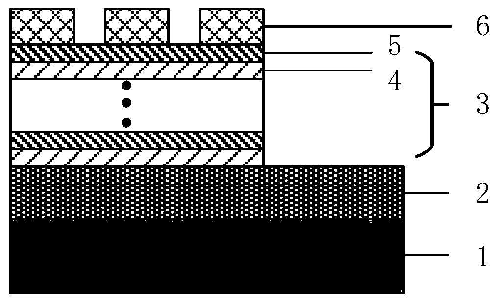
[0071] This embodiment provides a HfO 2 / Al 2 o 3 A superlattice memristor, the schematic diagram of which is shown in figure 1 As shown, it mainly includes a substrate 1 , a first electrode 2 , a superlattice memristor functional layer 3 and a second electrode 6 from bottom to top. Specific steps are as follows:

[0072] Step 1: Prepare the first electrode 2:

[0073] In the embodiment, TiN is selected as the first electrode 2, and a layer of the first electrode 2 is grown on a single crystal silicon sub...


PUM

PropertyMeasurementUnit
thicknessaaaaaaaaaa
thicknessaaaaaaaaaa

Abstract

The invention provides a superlattice memristor functional layer material, a memristor unit comprising the superlattice memristor functional layer and a manufacturing method thereof. The superlatticememristor functional layer material is a laminated structure formed by alternately stacking at least a first metal oxide layer and a second metal oxide layer in a first plane direction. In the invention, migration barriers of oxygen ions of two binary metal oxides are different so that a resistance state of the memristor can be stably and slowly changed under certain conditions, a modulation effect on an on-off state of an oxygen vacancy conductive filament is realized, and stability and consistency of the memristor are improved. Moreover, conductivity of the memristor can be continuously changed along with an external electric field so that a synaptic characteristic that the conductivity is continuously adjustable is realized, and synaptic linearity of cranial nerve-like morphology calculation is improved. The material, the unit and the method are of great significance to hardware implementation of storage fusion calculation and neuromorphic calculation.

Description

technical field [0001] The invention belongs to the technical field of microelectronic devices, and more specifically relates to a superlattice memristor and a preparation method thereof. Background technique [0002] Memristors are considered to be the fourth passive basic circuit element after resistors, capacitors, and inductors. The resistance value of a memristor changes with the amount of charge flowing through it, and it can maintain its resistance state when the current is turned off, thereby realizing the non-volatile information storage function. The research on the non-volatile information storage function of the memristor makes it applicable to high-density information storage or non-volatile state logic operation. In addition, some memristors have the characteristics of continuously adjustable conductance, which makes them also applicable to brain-like neuromorphic computing as synaptic devices. Memristors realize the fusion of storage and computing in a singl...

Claims


Application Information

Patent Timeline
Patent Type & Authority Applications(China)
IPC IPC(8): H01L45/00
CPCH10N70/883H10N70/041H10N70/8833
Inventor 王兴晟王成旭缪向水
Owner HUAZHONG UNIV OF SCI & TECH
Why Eureka
Try Eureka