Preparation method of epitaxial wafer for improving brightness of flip chip
A flip-chip and epitaxial wafer technology, applied in electrical components, circuits, semiconductor devices, etc., can solve the problems of ineffectiveness and reduced light extraction efficiency, and achieve the effect of improving light extraction efficiency, improving crystal quality, and improving brightness
- Summary
- Abstract
- Description
- Claims
- Application Information
AI Technical Summary
Problems solved by technology
Method used
Image
Examples
preparation example Construction
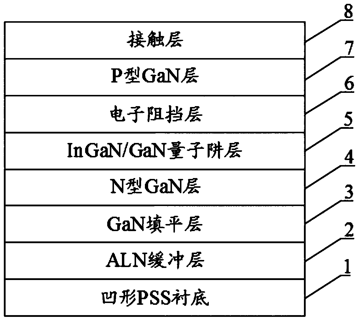
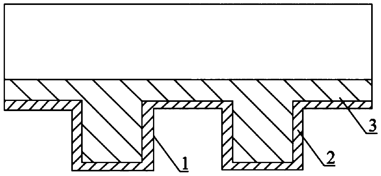
[0017] Please refer to Figure 1 to Figure 5 , a method for preparing an epitaxial wafer for improving the brightness of a flip-chip, comprising the steps of:
[0018] S1, sputtering a layer of ALN buffer layer on the concave PSS substrate;
[0019] S2 , growing a GaN filling layer on the ALN buffer layer using a high and low pressure environment, so as to fill up the concave PSS substrate.
[0020] As can be seen from the above description, the beneficial effects of the present invention are: since the PSS substrate adopts a sapphire substrate, the composition of the sapphire substrate is Al 2 o 3 , therefore, the GaN fill layer and the Al 2 o 3 A layer of ALN buffer layer is first grown between the sapphire substrates, and the ALN buffer layer acts as a link between the preceding and the following to improve the quality of crystal growth, so that the crystal surface and crystal quality rapidly grown on the concave PSS substrate are both good. It can reach the same level...
Embodiment 1
[0048] Please refer to Figure 1 to Figure 5 , Embodiment 1 of the present invention is:
[0049]A method for preparing an epitaxial wafer for improving the brightness of a flip-chip, comprising the steps of:
[0050] S1, sputtering a layer of ALN buffer layer 2 on the concave PSS substrate 1;
[0051] S2 , growing a GaN leveling layer 3 on the ALN buffer layer 2 using a high and low pressure environment to fill up the concave PSS substrate 1 , and using the ALN buffer layer 2 to enable rapid growth of the GaN leveling layer 3 .
[0052] S3, continue to grow the N-type GaN layer 4 on the flat GaN filling layer 3;
[0053] S4. Continue growing the InGaN / GaN quantum well layer 5, the electron blocking layer 6 and the P-type GaN layer 7 on the N-type GaN layer 4;
[0054] S5. Finally, a contact layer 8 is grown on the P-type GaN layer 7 to obtain a flip-chip epitaxial wafer.
[0055] In this embodiment, the ALN buffer layer 2 plays a connecting role, so that the surface and c...
Embodiment 2
[0057] Please refer to Figure 1 to Figure 5 , the second embodiment of the present invention is:
[0058] A method for preparing epitaxial wafers for improving the brightness of flip-chips. On the basis of the first embodiment above, step S1 is specifically:
[0059] S1, carry out the ALN sputtering buffer layer process on the concave PSS substrate 1, to generate a 30nm thick ALN buffer layer 2, the sputtering pressure of the ALN sputtering buffer layer process is 50torr, and the sputtering temperature is 500 °, The power is set to 3KV, and the input includes 15% Ar, 5% O 2 and 80% of N 2 The mixed gas, where, N 2 Participate in the generation of ALN buffer layer 2, Ar and O 2 It plays a catalytic role to accelerate the formation of the ALN buffer layer 2, and the formation rate of the ALN buffer layer 2 under this condition can reach 20um / h.
[0060] In this embodiment, step S2 is specifically:
[0061] S21. First perform a low-pressure lateral growth process on the AL...
PUM
| Property | Measurement | Unit |
|---|---|---|
| thickness | aaaaa | aaaaa |
Abstract
Description
Claims
Application Information
 - R&D
- Intellectual Property
- Life Sciences
- Materials
- Tech Scout
- Unparalleled Data Quality
- Higher Quality Content
- 60% Fewer Hallucinations
Browse by: Latest US Patents, China's latest patents, Technical Efficacy Thesaurus, Application Domain, Technology Topic, Popular Technical Reports.
© 2025 PatSnap. All rights reserved.Legal|Privacy policy|Modern Slavery Act Transparency Statement|Sitemap|About US| Contact US: help@patsnap.com


