Simulation method for strain regulation and control of selenium disulfide semiconductor device
A technology of selenium disulfide and simulation method, which is applied in the fields of instruments, special data processing applications, electrical digital data processing, etc.
- Summary
- Abstract
- Description
- Claims
- Application Information
AI Technical Summary
Problems solved by technology
Method used
Image

Examples
Embodiment Construction
[0018] The present invention will be further described below in conjunction with the accompanying drawings.
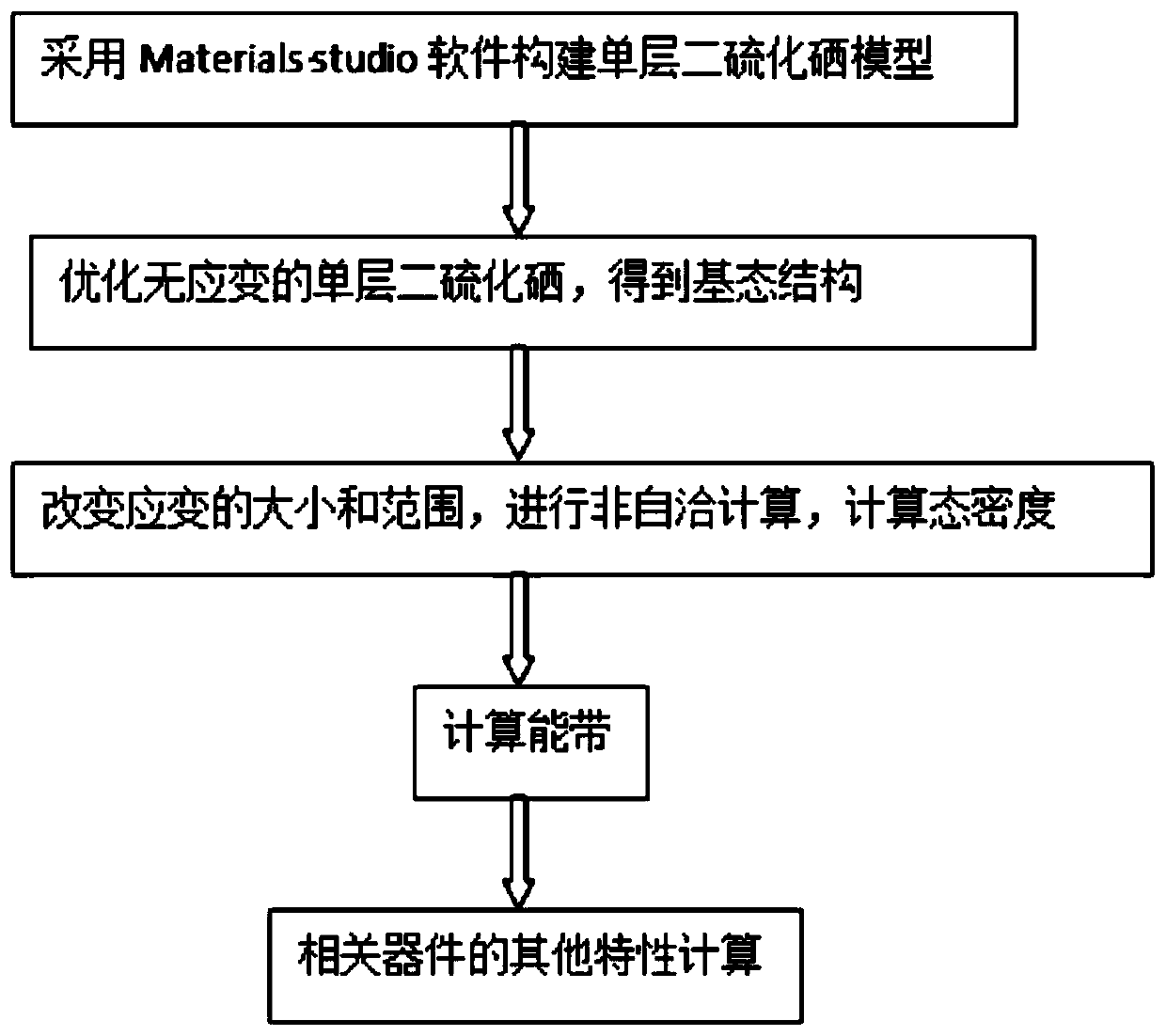
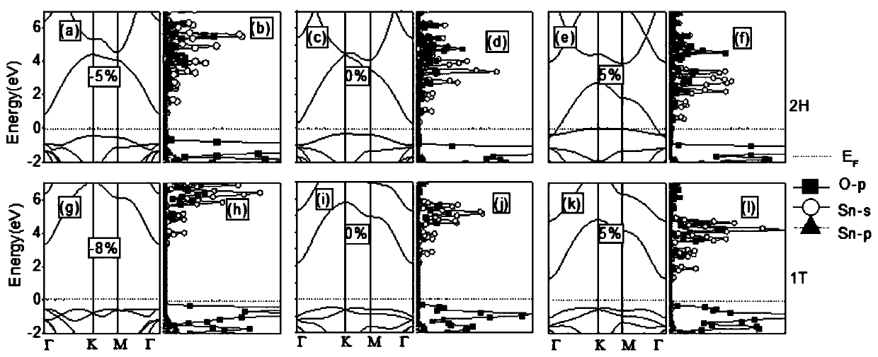
[0019] Such as figure 1 Shown is a schematic flow chart of the simulation method for strain-regulated selenium disulfide semiconductor devices, including the following steps: use Materials Studio software to construct a single-layer selenium disulfide model → optimize the unstrained single-layer selenium sulfide-free to obtain the ground state structure → change the strained Size and range, perform non-self-consistent calculations → calculate the density of states, calculate energy bands → calculate other characteristics of related devices.
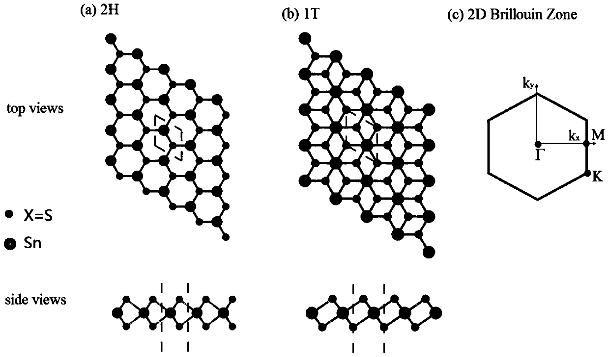
[0020] Using Materials Studio software to build a single-layer selenium disulfide model, including the following steps: selenium disulfide has three atomic planes, the Sn atomic plane in the middle separates the S atoms of the two hexagonal side planes, and the adjacent layers are separated by van der Waals force Combine with lay...
PUM
 Abstract
Description
Claims
Application Information