

Resistance-type flexible pressure sensor and preparation method thereof
A pressure sensor and resistive technology, applied in the field of resistive flexible pressure sensor and its preparation, can solve the problems of difficult control of process parameters, cumbersome steps, many materials, etc., and achieve the effects of low cost, simple process and improved sensitivity
- Summary
- Abstract
- Description
- Claims
- Application Information
AI Technical Summary
Problems solved by technology
Method used
Image

Examples
preparation example Construction
[0030] The preparation method of the resistive flexible pressure sensor provided by the present invention comprises:
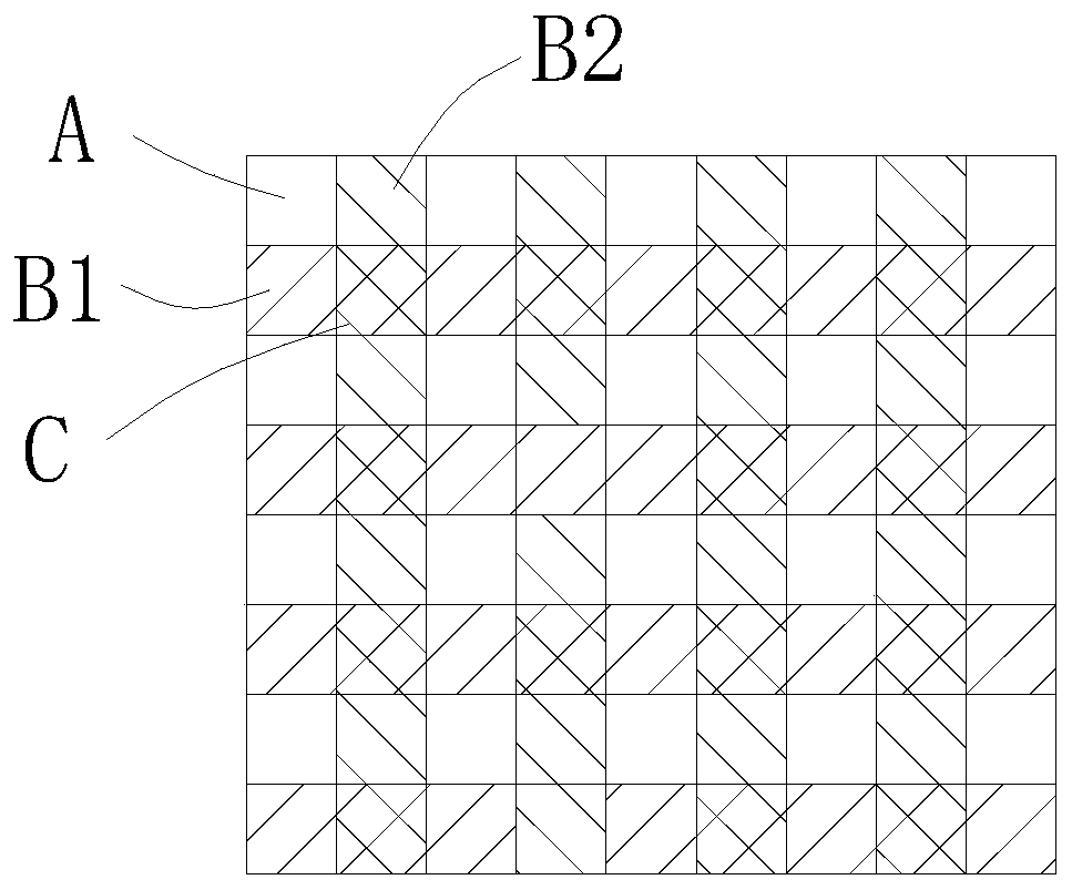
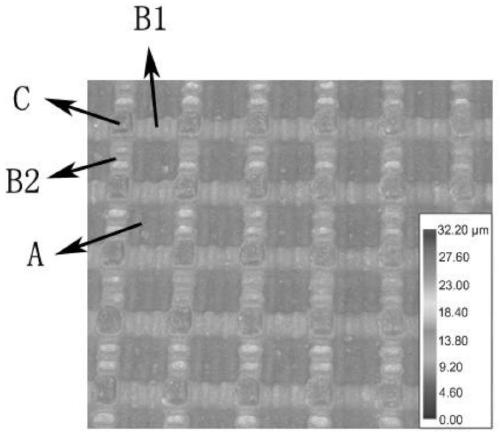
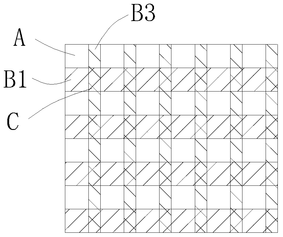
[0031] S1, providing a first flexible substrate, using a laser to etch a surface of the first flexible substrate to form microstructures of at least two heights;
[0032] S2, forming a conductive layer on the surface of the first flexible substrate with the microstructure to obtain a first flexible substrate;
[0033] S3, providing a second flexible substrate, wherein the second flexible substrate includes a second flexible substrate and electrodes disposed on a surface of the second flexible substrate; and
[0034] S4, stacking the second flexible substrate on the first flexible substrate, and making the electrodes contact part of the conductive layer to obtain a resistive flexible pressure sensor.
[0035] In step S1, the thickness of the first flexible substrate is 50 μm to 200 μm, and the material of the first flexible substrate is an insulating polymer m...
Embodiment 1
[0080] (1) Weigh 1g of polydimethylsiloxane (PDMS) prepolymer into a beaker, then measure 0.1g of curing agent into the beaker and stir evenly, and place it under 0.1Torr vacuum condition for 10min to remove air bubbles. Select a piece of clean glass substrate, spin-coat the above mixed solution on its surface at a rotation speed of 500rpm for 10s, and cure it at 60°C to obtain a first flexible substrate and a second flexible substrate with a thickness of 100 μm.
[0081] (2) A pulsed laser with a wavelength of 355nm and a pulse width of 500fs is used to etch a grid pattern on the surface of the first flexible substrate, the horizontal and vertical grid filling intervals are both 20 microns, the single pulse energy of the laser is 10 μJ, and the scanning speed is 500mm / s, three height microstructures are obtained after etching.
[0082] (3) Prepare an AgNWs ethanol solution with a concentration of 10 mg / mL, treat the surface of the microstructure with oxygen plasma, then spin-...
PUM
| Property | Measurement | Unit |
|---|---|---|
| Thickness | aaaaa | aaaaa |
| Wavelength | aaaaa | aaaaa |
Abstract
Description
Claims
Application Information