Silicon carbide single crystal, substrate and preparation method thereof

A silicon carbide single crystal and crystal growth technology, applied in chemical instruments and methods, single crystal growth, single crystal growth and other directions, can solve the axial temperature gradient drop, difficult to achieve the radial temperature gradient of silicon carbide single crystal, change, etc. question

Active Publication Date: 2020-04-28
SICC CO LTD
View PDF5 Cites 3 Cited by
  • Summary
  • Abstract
  • Description
  • Claims
  • Application Information

AI Technical Summary

Problems solved by technology

The existing induction coil heating method, on the one hand, is difficult to increase the axial temperature gradient of the growth chamber without affecting the radial temperature gradient and ensure a small radial temperature gradient; on the other hand, when reducing the radial temperature gradient , the axial temperature gradient also has a larg

Method used


Image

  • Silicon carbide single crystal, substrate and preparation method thereof
  • Silicon carbide single crystal, substrate and preparation method thereof
  • Silicon carbide single crystal, substrate and preparation method thereof

Examples


Embodiment 1

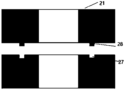
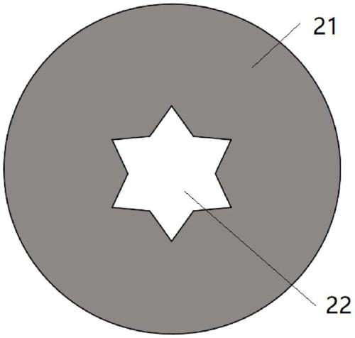
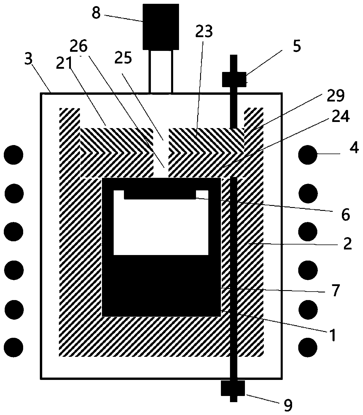
[0077] refer to figure 1 , the crystal growth device, which includes a crucible 1, an insulating layer 2, a furnace body 3 and a heating element 4, the insulating layer 2 includes an upper insulating layer group 21 above the crucible 1, and the upper insulating layer group 21 is provided with a temperature measuring hole 22, and the upper insulating layer group 21 is provided with a temperature measuring hole 22. The insulation layer group 21 comprises the first upper insulation layer 23 and the second upper insulation layer 24 of the common central axis, the first upper insulation layer 23 is provided with the first opening 25, the second upper insulation layer 24 is provided with the second opening 26, and the temperature measuring hole 22 make the crucible 1 form a low-temperature zone for holding the raw material 7 and a high-temperature zone for setting the seed crystal 6; it also includes a rotation adjustment mechanism 5, and the rotation adjustment mechanism rotates the...

Embodiment 2

[0088] The crystal growth device also includes a lifting adjustment mechanism 9; the lifting adjustment structure includes a second motor, a lifting rod and a second connector, and the second connector is connected with the first upper insulation layer 23 and / or the second upper insulation layer 24, and the second Connect the motor to drive the first upper insulation layer 23 and / or the second upper insulation layer 24 to lift along the common central axis through the lifting rod and the second connector; the insulation layer 2 includes the side insulation layer 2, the height of the lifting of the upper insulation layer group Not higher than the height of the side insulation layer 2. The crystal growth device can adjust the radial temperature gradient in the growth chamber for growing single crystals; while reducing the radial temperature gradient, it can also ensure a certain axial temperature gradient, and can efficiently produce high-quality, low-defect single crystal.

[...

Embodiment 3

[0093] refer to Figure 4 , as an embodiment, the crystal growth device includes a crucible 1, a heating coil group and a heat preservation structure, the crucible 1 forms a growth chamber, and the growth chamber includes a raw material 7 area containing a raw material 7 and a crystal growth area where a seed crystal 6 is set, and the heating The coil set is arranged around the side wall of the crucible 1, and the heating coil set includes a first coil set corresponding to the height of the raw material 7 area and a second coil set corresponding to the height of the crystal growth area, along the path from the raw material 7 to the seed crystal 6 direction, the inner diameter of the second coil group increases. The coil diameter is increased from the raw material 7 upwards, thereby reducing the temperature at the seed crystal 6. Compared with the previous coil design with a constant diameter, the axial temperature gradient in the growth chamber is increased. However, for the s...


PUM


Abstract

The invention discloses a silicon carbide single crystal, a substrate and a preparation method thereof, which belongs to the field of semiconductor materials. The preparation method of the silicon carbide single crystal comprises the following steps: forming a low-temperature region and a high-temperature region in a crucible by virtue of a temperature measuring hole formed in an upper thermal insulation layer group outside the crucible, and transmitting a raw material gas phase in the low-temperature region to the surface of a seed crystal in the high-temperature region by virtue of a physical gas phase transmission method to grow the crystal; wherein the upper heat preservation layer set comprises a second heat preservation layer and a first heat preservation layer which are sequentiallyarranged in the seed crystal direction of raw materials. The first heat preservation layer is provided with a first opening, the second heat preservation layer is provided with a second opening, anda rotary adjusting mechanism rotates the first heat preservation layer and/or the second heat preservation layer to adjust the cross sectional area of a temperature measuring hole formed by the firstopening and the second opening, so that the axial and radial temperature gradient in the crucible in the crystal growth process is adjusted. According to the preparation method of the silicon carbidesingle crystal, the radial temperature gradient in a growth cavity for growing the single crystal can be adjusted; and while the radial temperature gradient is reduced, a certain axial temperature gradient is ensured, and the high-quality silicon carbide single crystal is efficiently prepared.

Description

technical field [0001] The application relates to a silicon carbide single crystal, a substrate and a preparation method thereof, belonging to the field of semiconductor materials. Background technique [0002] Silicon carbide single crystal is one of the most important third-generation semiconductor materials. It is widely used in power electronics, RF devices, optoelectronic devices and other fields. [0003] At present, the main preparation method of silicon carbide single crystal is physical vapor transport (PVT) method. In the process of preparing single crystal by PVT method, there are radial temperature gradient and axial temperature gradient in the growth chamber of growing single crystal. In the stable growth stage of single crystal, a larger axial temperature gradient has a faster single crystal growth rate, and a smaller radial temperature gradient can reduce the introduction of stress and dislocation. However, it is difficult to simultaneously achieve a large ...

Claims


Application Information

Patent Timeline
IPC IPC(8): C30B23/00C30B29/36
CPCC30B23/002C30B29/36
Inventor 方帅高宇晗高超李霞宁秀秀王路平张九阳王宝玉杨晓俐潘亚妮舒天宇
Owner SICC CO LTD
Why Eureka
Try Eureka