Printing screen for heterojunction solar cell and printing method thereof
A technology of solar cells and printing methods, applied in printing, printing presses, rotary printing presses, etc., can solve the problems of non-conduction of main and auxiliary grids, battery fragment grids, affecting photo-generated current collection, etc., to increase battery efficiency and increase photo-generated current. The effect of current collection
- Summary
- Abstract
- Description
- Claims
- Application Information
AI Technical Summary
Problems solved by technology
Method used
Image

Examples
Embodiment 1
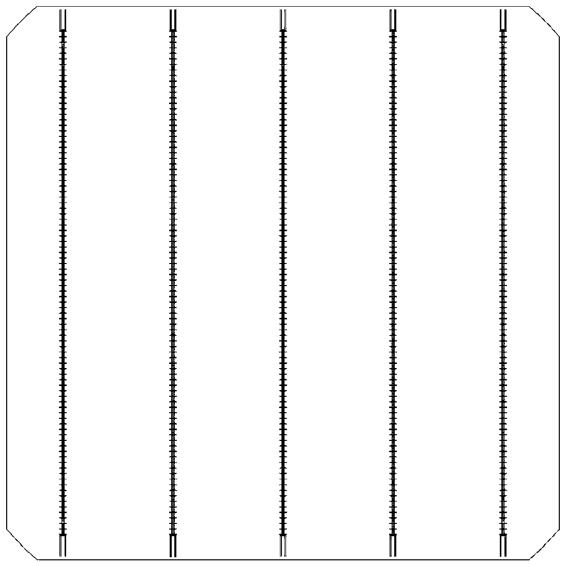
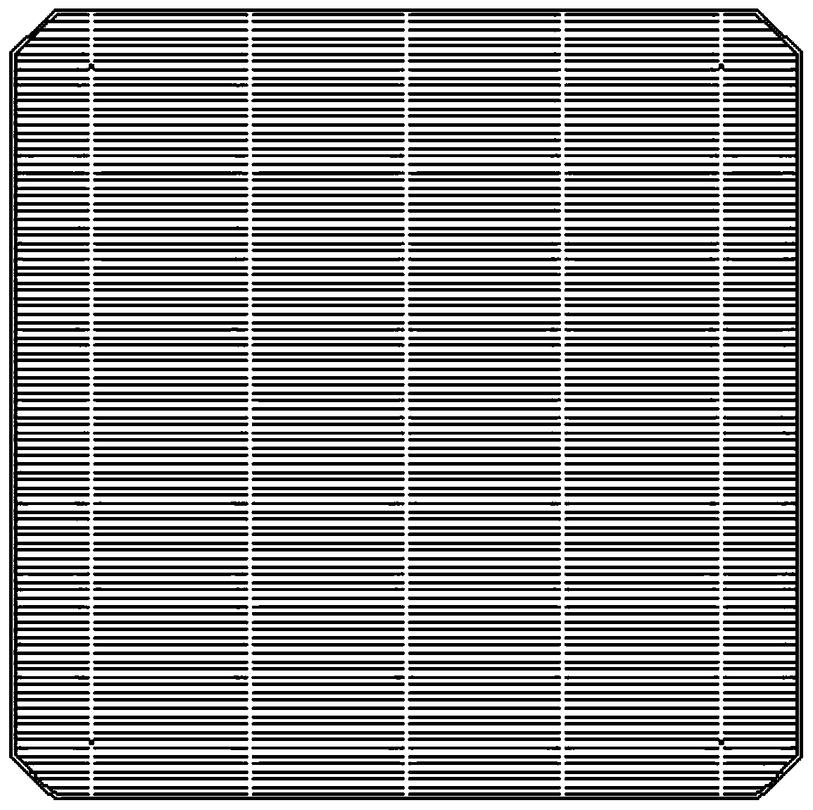
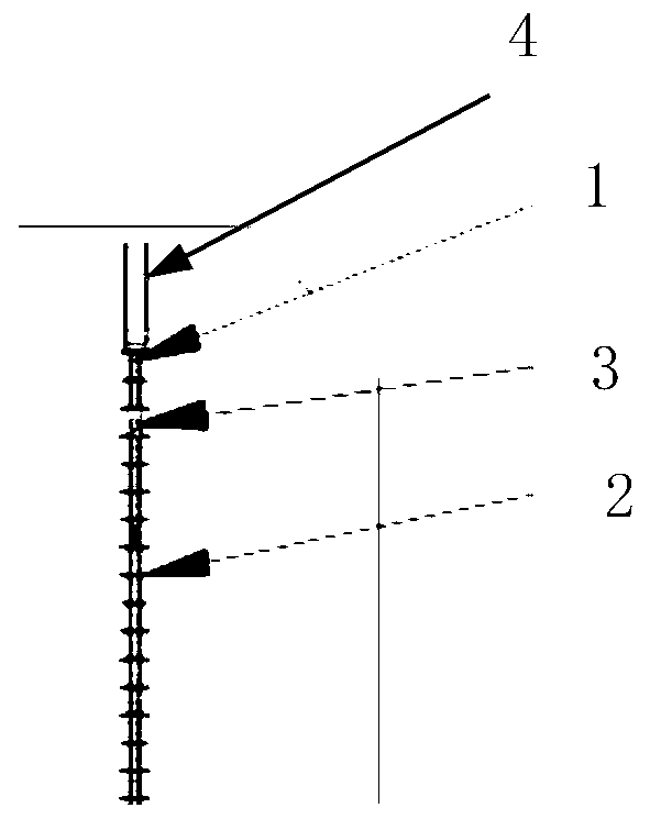
[0037] A printing screen for heterojunction solar cells and a printing method thereof, specifically comprising the following steps:
[0038] (1) Perform texturing treatment on N-type monocrystalline silicon wafers with a thickness of 170 μm to form a pyramid textured surface, remove impurity ions and clean the surface;
[0039] (2) Prepare the double intrinsic amorphous silicon layer and the doped amorphous silicon layer on the front and back by plasma chemical vapor deposition. The thickness of amorphous silicon is 20nm;
[0040] (3) Deposit the ITO film by magnetron sputtering, the thickness of the ITO film on the front and back is 100nm, and the silicon chip is supported on the carrier to form a mask design, and the mask width is 1.5mm.
[0041] (4) The back silver metal electrode is formed by step-by-step screen printing, the width of the main grid is 1 mm, the number of the main grid is 5, the line width of the auxiliary grid is 30 μm, and the number of auxiliary grids i...
Embodiment 2
[0045] A printing screen for heterojunction solar cells and a printing method thereof, specifically comprising the following steps:
[0046] (1) Perform texturing treatment on N-type monocrystalline silicon wafers with a thickness of 170 μm to form a pyramid textured surface, remove impurity ions and clean the surface;
[0047](2) Prepare the double intrinsic amorphous silicon layer and the doped amorphous silicon layer on the front and back by plasma chemical vapor deposition. The thickness of amorphous silicon is 20nm;
[0048] (3) Deposit the ITO film by magnetron sputtering, the thickness of the ITO film on the front and back is 100nm, and the silicon chip is supported on the carrier to form a mask design, and the mask width is 1.5mm.
[0049] (4) The back silver metal electrode is formed by step-by-step screen printing, the width of the main grid is 1 mm, the number of the main grid is 5, the line width of the auxiliary grid is 30 μm, and the number of auxiliary grids is...
Embodiment 3
[0053] A printing screen for heterojunction solar cells and a printing method thereof, specifically comprising the following steps:
[0054] (1) Perform texturing treatment on N-type monocrystalline silicon wafers with a thickness of 170 μm to form a pyramid textured surface, remove impurity ions and clean the surface;
[0055] (2) Prepare the double intrinsic amorphous silicon layer and the doped amorphous silicon layer on the front and back by plasma chemical vapor deposition. The thickness of amorphous silicon is 20nm;
[0056] (3) Deposit the ITO film by magnetron sputtering, the thickness of the ITO film on the front and back is 100nm, and the silicon chip is supported on the carrier to form a mask design, and the mask width is 1.5mm.
[0057] (4) The back silver metal electrode is formed by step-by-step screen printing, the width of the main grid is 1 mm, the number of the main grid is 5, the line width of the auxiliary grid is 30 μm, and the number of auxiliary grids i...
PUM
| Property | Measurement | Unit |
|---|---|---|
| width | aaaaa | aaaaa |
| length | aaaaa | aaaaa |
| length | aaaaa | aaaaa |
Abstract
Description
Claims
Application Information
 - R&D
- Intellectual Property
- Life Sciences
- Materials
- Tech Scout
- Unparalleled Data Quality
- Higher Quality Content
- 60% Fewer Hallucinations
Browse by: Latest US Patents, China's latest patents, Technical Efficacy Thesaurus, Application Domain, Technology Topic, Popular Technical Reports.
© 2025 PatSnap. All rights reserved.Legal|Privacy policy|Modern Slavery Act Transparency Statement|Sitemap|About US| Contact US: help@patsnap.com