Millimeter wave MMIC heat dissipation package based on 3D heterogeneous integration technology

A millimeter-wave, heterogeneous technology, applied in electrical components, electrical solid devices, circuits, etc., can solve the problem of inability to take into account the millimeter-wave radio frequency front-end chip millimeter-wave microwave performance and heat conduction, limit the engineering application of millimeter-wave radio frequency front-end chips, and millimeter-wave radio frequency front-end chips. The microwave radio frequency front-end chip has the effect of shortening the interconnect size, ensuring electrical performance, and high yield.

Inactive Publication Date: 2020-05-08
CETC GUOJI SOUTHERN GRP CO LTD
6 Cites 2 Cited by

AI-Extracted Technical Summary

Problems solved by technology

[0003] In the traditional low-cost plastic package, two forms of wire bonding (Wire Bonding) and bumping flip-chip (Bumping Flip-chip) are mainly used to interconnect the chip and the package substrate; Since the interconnection lead is equivalent to a large inductance connected in series with the input and output terminals of the RF front-end chip in the millimeter wave frequency band, the impedance mismatch between the input and output terminals of the millimeter wave RF front-end chip will seriously affect the electrical performance of the RF chip.
For the Bumping Flip-chip interconnection form, on the one hand, the front side of the RF chip is facing down, and the distance between the circuit o...

Method used

In the present invention, the back side of GaAs MMIC is bonded with high thermal conductivity metal block by high thermal conductivity conductive glue, the s...

Abstract

The invention discloses a millimeter wave MMIC heat dissipation package based on a 3D heterogeneous integration technology. The millimeter wave MMIC heat dissipation package comprises a package substrate, a transmission line arranged on the lower surface of the packaging substrate, a TSV via hole arranged in the packaging substrate, a transmission line arranged on the upper surface of the packaging substrate, gold bumps, a millimeter wave GaAs MMIC, a metal PAD arranged on the surface of the GaAs MMIC, a millimeter wave circuit pattern arranged on the surface of the GaAs MMIC, a cavity in theupper surface of the packaging substrate, a high-thermal-conductivity bonding material, a heat dissipation metal block, a plastic packaging material and a BGA solder ball. The millimeter wave MMIC heat dissipation package has the advantages of being small in size, light in weight, low in cost, good in millimeter wave electrical characteristic, excellent in heat dissipation performance and the like, and can be widely applied to a millimeter wave radio frequency front-end system.

Application Domain

Semiconductor/solid-state device detailsSolid-state devices +1

Technology Topic

Radio frequencyThermal transmittance +10

Image

  • Millimeter wave MMIC heat dissipation package based on 3D heterogeneous integration technology
  • Millimeter wave MMIC heat dissipation package based on 3D heterogeneous integration technology
  • Millimeter wave MMIC heat dissipation package based on 3D heterogeneous integration technology

Examples

  • Experimental program(1)

Example Embodiment

[0026] Example
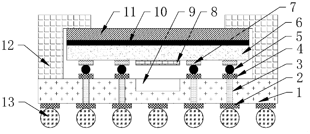
[0027] like figure 1 As shown, a millimeter-wave MMIC heat dissipation package based on 3D heterogeneous integration technology includes a packaging substrate 1, a transmission line 2 on the lower surface of the packaging substrate, a TSV via 3 arranged inside the packaging substrate, a transmission line 4 on the upper surface of the packaging substrate, and gold bumps. Point 5, millimeter wave GaAs MMIC6, metal PAD7 set on the surface of GaAs MMIC, millimeter wave circuit pattern 8 set on the surface of GaAs MMIC, cavity on the upper surface of the package substrate 9, high thermal conductivity adhesive material 10, heat dissipation metal block 11, Plastic encapsulation material 12 and BGA solder ball 13;
[0028] The transmission line 2 on the lower surface of the packaging substrate is connected to the transmission line 4 on the upper surface of the packaging substrate through the TSV via hole 3 provided inside the packaging substrate;
[0029] The GaAs MMIC6 is flipped face-down (Flip-chip) on the upper surface of the packaging substrate 1, and the transmission line 4 on the upper surface of the packaging substrate is interconnected with the metal PAD7 arranged on the surface of the GaAs MMIC through Au Bumping; in addition, the millimeters arranged on the surface of the GaAs MMIC The area where the wave circuit pattern 8 is located needs to correspond to the cavity 9 on the upper surface of the packaging substrate.
[0030] The heat dissipation metal block 11 is bonded to the back of the GaAs MMIC through a high thermal conductivity bonding material 10 .
[0031] The BGA solder balls 13 are located on the lower surface of the packaging substrate 1 and are arranged on the transmission line 2 on the lower surface of the packaging substrate.
[0032] Plastic encapsulation material 12 is used to encapsulate the package as a whole, but heat dissipation metal block 11 cannot be completely encapsulated by plastic encapsulation material 12, and its upper surface needs to be exposed to the air in a large area, and the exposed area is more than half of the heat dissipation metal Block 11 area.
[0033] GaAs MMIC6 is a millimeter wave RF front-end transceiver chip.
[0034] The package can be applied to the package of the millimeter-wave RF front-end transceiver MMIC with a frequency band below the Ka band and a power below 2W.
[0035] The packaging substrate is a silicon-based TSV adapter board with an aspect ratio of 200:30. Based on semiconductor process processing, the transmission line on the upper surface of the packaging substrate, the transmission line on the lower surface of the packaging substrate, the TSV vias inside the packaging substrate, and the cavity on the upper surface of the packaging substrate body for processing.
[0036]In the present invention, the gold bumps are bonded to the PAD provided on the surface of the GaAs MMIC by using the thermocompression ultrasonic process, and then the GaAs MMIC is reversed on the surface of the package substrate through the inversion process with the thermocompression ultrasonic function, so as to realize the arrangement on the surface of the GaAs MMIC The interconnection between the PAD and the surface transmission line on the package substrate.
[0037] In the present invention, the back of the GaAs MMIC is bonded with a high thermal conductivity metal block with a high thermal conductivity conductive adhesive. The size of the heat conduction metal block is equivalent to that of the GaAs MMIC to ensure the heat dissipation area, and the thickness is 0.1 mm to avoid the risk of supporting stress.
[0038] The present invention adopts plastic encapsulation material for packaging and encapsulation, but the encapsulation material only encloses the surroundings of the heat-conducting metal block, and the upper surface of the heat-conducting metal block needs to be exposed to the air in a large area so as to form good heat convection with the air, ensuring GaAs MMIC works properly.
[0039] like figure 2 As shown, the gain versus frequency diagram of this embodiment covers the 5G millimeter wave frequency band, that is, 24-28 GHz, and the electrical performance after packaging is in good agreement with the electrical performance of the bare chip before packaging, and better millimeter wave electrical performance can be achieved. performance.

PUM

PropertyMeasurementUnit
Thickness0.2mm

Description & Claims & Application Information

We can also present the details of the Description, Claims and Application information to help users get a comprehensive understanding of the technical details of the patent, such as background art, summary of invention, brief description of drawings, description of embodiments, and other original content. On the other hand, users can also determine the specific scope of protection of the technology through the list of claims; as well as understand the changes in the life cycle of the technology with the presentation of the patent timeline. Login to view more.

Similar technology patents

Aminopyrine production method

InactiveCN101891683Areduce lossreduce losses
Owner:JIHENG PHARMA HENGSHUI CITY

Classification and recommendation of technical efficacy words

Why Eureka
Try Eureka