Organic light-emitting diode and preparation method thereof

A light-emitting diode and organic technology, applied in semiconductor/solid-state device manufacturing, electrical components, electric solid-state devices, etc., can solve the problems of complicated preparation procedures and poor packaging effect of OLED light-emitting devices, and achieve simple process, improved service life, The effect of low production cost

Active Publication Date: 2020-05-08
WUHAN CHINA STAR OPTOELECTRONICS SEMICON DISPLAY TECH CO LTD
View PDF2 Cites 0 Cited by
  • Summary
  • Abstract
  • Description
  • Claims
  • Application Information

AI Technical Summary

Problems solved by technology

[0004] The object of the present invention is to provide an organic light-emitting diode and its preparation method to solve the problems of poor encapsulation effect and complicated preparation procedures of OLED light-emitting devices in the prior art.

Method used


Image

  • Organic light-emitting diode and preparation method thereof
  • Organic light-emitting diode and preparation method thereof
  • Organic light-emitting diode and preparation method thereof

Examples


Embodiment 1

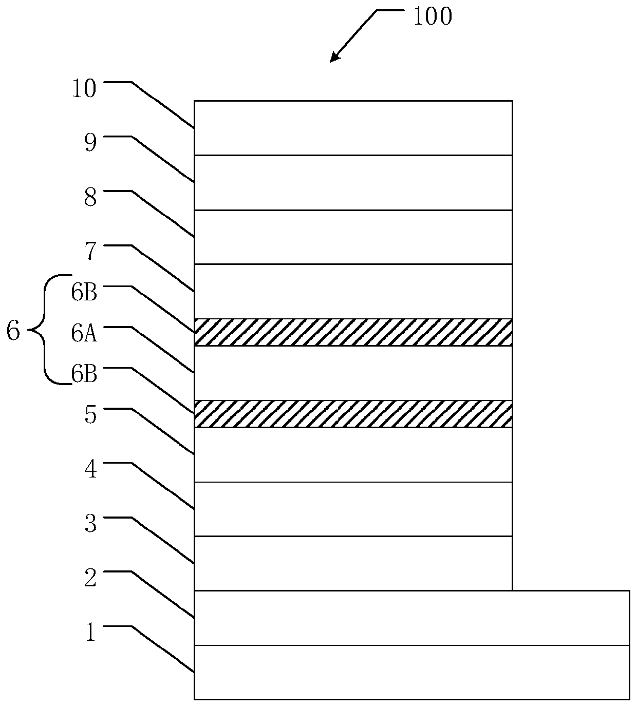
[0038] An organic light emitting diode 100 is disclosed in the embodiment of the present invention, such as figure 1 As shown, the organic light emitting diode 100 includes a substrate layer 1, a first electrode layer 2, a hole injection layer 3, a hole transport layer 4, an electron blocking layer 5, a blending active layer 6, a hole blocking layer 7, Electron transport layer 8 , electron injection layer 9 and second electrode layer 10 .

[0039] The material of the substrate layer 1 is polyimide (Polyimide, PI), which is a flexible substrate layer 1, which protects the structure of the organic light emitting diode 100 and enables the organic light emitting diode 100 to realize flexible display.

[0040] The first electrode layer 2 is arranged on the substrate layer 1, and the material of the first electrode layer 2 is indium tin oxide (ITO), which is used to provide a current and voltage for the organic light emitting diode 100 to promote hole Migrate to the luminescent lay...

Embodiment 2

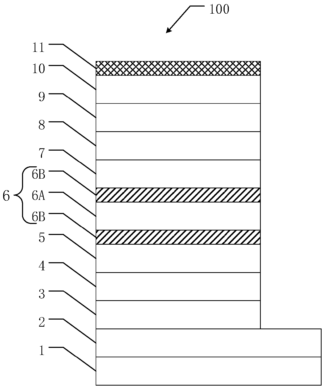
[0065] An organic light emitting diode 100 is disclosed in the embodiment of the present invention, such as image 3 As shown, the organic light emitting diode 100 includes a substrate layer 1, a first electrode layer 2, a hole injection layer 3, a hole transport layer 4, an electron blocking layer 5, a blending active layer 6, a hole blocking layer 7, The electron transport layer 8 , the electron injection layer 9 , the second electrode layer 10 and the second encapsulation layer 11 .

[0066] The material of the substrate layer 1 is polyimide (Polyimide, PI), which is a flexible substrate layer 1, which protects the structure of the organic light emitting diode 100 and enables the organic light emitting diode 100 to realize flexible display.

[0067] The first electrode layer 2 is arranged on the substrate layer 1, and the material of the first electrode layer 2 is indium tin oxide (ITO), which is used to provide a current and voltage for the organic light emitting diode 100...


PUM

PropertyMeasurementUnit
transmittivityaaaaaaaaaa

Abstract

The invention provides an organic light-emitting diode and a preparation method thereof. According to the invention, the packaging is performed on the surface of a light-emitting layer, so the processis simple, the light-emitting layer can be effectively protected, the activity of the light-emitting layer material is prevented from being reduced due to corrosion caused by water and oxygen invasion, and the service life of the organic light-emitting diode is effectively prolonged. The problems that in the prior art, an organic light-emitting device is poor in packaging effect, complex in preparation procedure and the like are solved.

Description

technical field [0001] The invention relates to the display field, in particular to an organic light emitting diode and a preparation method thereof. Background technique [0002] OLED (Organic Light-Emitting Diode, Organic Light-Emitting Diode) is an emerging flat panel display technology. OLED display technology is different from traditional LCD display methods. It does not require a backlight and uses very thin organic material coatings and glass substrate layers. When an electric current passes through, these organic materials will emit light. Because of its simple preparation process, low cost, low power consumption, high luminous brightness, wide range of working temperature, light and thin volume, fast response speed, easy to realize color display and large screen display, easy to realize and match with integrated circuit driver, It is easy to realize the advantages of flexible display, so it has broad application prospects. [0003] Under the action of an external ...

Claims


Application Information

Patent Timeline
Patent Type & Authority Applications(China)
IPC IPC(8): H01L51/56H01L51/52
CPCH10K50/84H10K50/844H10K71/00H10K71/12H10K50/80H10K50/00
Inventor 钟安星
Owner WUHAN CHINA STAR OPTOELECTRONICS SEMICON DISPLAY TECH CO LTD
Why Eureka
Try Eureka