Organic white light emitting device based on stepped multi-reflection intersystem crossing process and preparation method thereof

A light-emitting device, a stepped technology, applied in semiconductor/solid-state device manufacturing, electric solid-state devices, semiconductor devices, etc., can solve the problems of low efficiency of all-fluorescent white light devices, reduce manufacturing costs, and roll-off efficiency, so as to improve luminous efficiency , reduce the preparation cost and improve the utilization rate

Active Publication Date: 2020-05-15
UNIV OF ELECTRONICS SCI & TECH OF CHINA
View PDF7 Cites 0 Cited by
  • Summary
  • Abstract
  • Description
  • Claims
  • Application Information

AI Technical Summary

Problems solved by technology

[0005] The invention provides an organic white light-emitting device based on a stepped multi-reaction intersystem crossing process and a preparation method thereof, which solves the problems of low efficiency, poor stability, and serious efficiency roll-off of an all-fluorescent white light device, and the device has no heavy metals, Reduced preparation costs

Method used


Image

  • Organic white light emitting device based on stepped multi-reflection intersystem crossing process and preparation method thereof
  • Organic white light emitting device based on stepped multi-reflection intersystem crossing process and preparation method thereof
  • Organic white light emitting device based on stepped multi-reflection intersystem crossing process and preparation method thereof

Examples


Embodiment 1

[0043] Embodiment 1: control group

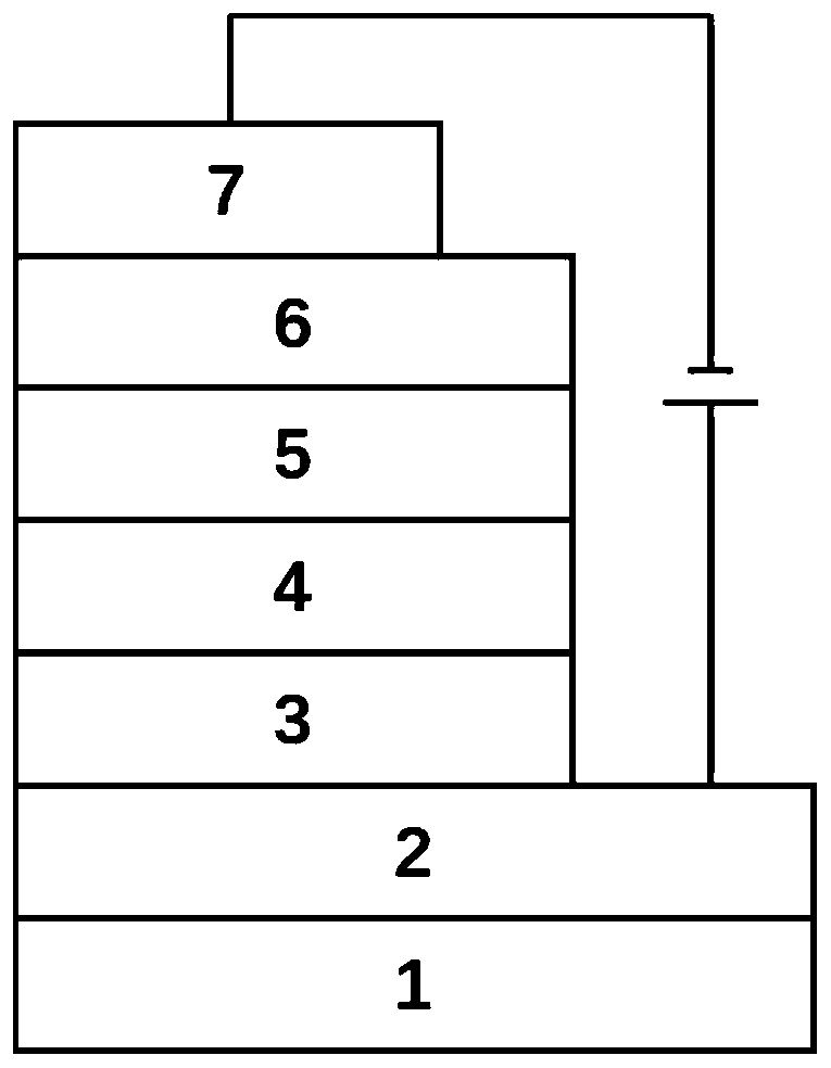
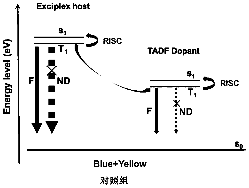
[0044] Clean the substrate composed of the substrate and the transparent conductive anode ITO, put it in a vacuum drying oven to dry after cleaning; put it in the evaporation chamber, and pump the vacuum to 3×10 -4 Pa and below, evaporate a hole transport layer with a thickness of 35nm, and evaporate a light-emitting layer on the hole transport layer (the light-emitting layer adopts ternary co-evaporation, and its ratio is controlled by the calculated rate, and the structure is traditional. The guest structure has an anti-intersystem crossing process, the materials used are MCP, 4CzPNPh, PO-T2T, the ratio of mass content is 1:0.005:1, and the thickness is 30nm), and the electron transport layer (thickness is 40nm), vapor-deposits a metal cathode (thickness is 120nm) on the electron transport layer, wherein, the evaporation rate of the organic layer is The metal cathode evaporation rate is

Embodiment 2

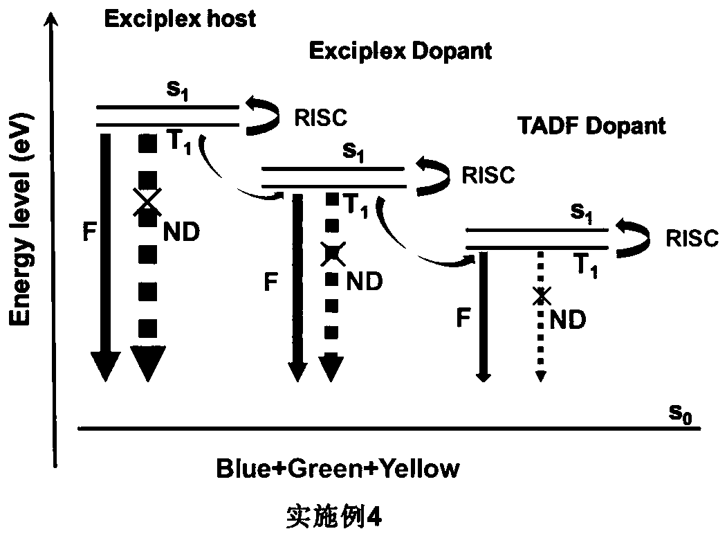
[0046]Clean the substrate composed of the substrate and the transparent conductive anode ITO, put it in a vacuum drying oven to dry after cleaning; put it in the evaporation chamber, and pump the vacuum to 3×10 -4 Pa and below, evaporate a hole transport layer with a thickness of 35nm, and evaporate a light-emitting layer on the hole transport layer (the light-emitting layer adopts ternary co-evaporation, the ratio is controlled by the calculated rate, and the structure is traditional The host-guest structure has two anti-intersystem crossing processes, the materials used are MCP, 4CzPNPh, PO-T2T, the mass content ratio is 1:0.003:1, and the thickness is 30nm), and the electron transport is evaporated on the light-emitting layer layer (thickness is 40nm), evaporate metal cathode (thickness is 120nm) on electron transport layer, wherein, organic layer evaporation rate is The metal cathode evaporation rate is

Embodiment 3

[0048] Clean the substrate composed of the substrate and the transparent conductive anode ITO, put it in a vacuum drying oven to dry after cleaning; put it in the evaporation chamber, and pump the vacuum to 3×10 -4 Pa and below, evaporate a hole transport layer with a thickness of 35nm, and evaporate a light-emitting layer on the hole transport layer (the light-emitting layer adopts ternary co-evaporation, the ratio is controlled by the calculated rate, and the structure is traditional The host-guest structure has two anti-intersystem crossing processes, the materials used are MCP, 4CzPNPh, PO-T2T, the mass content ratio is 1:0.005:1, and the thickness is 30nm), and the electron transport is evaporated on the light-emitting layer layer (thickness is 40nm), evaporate metal cathode (thickness is 120nm) on electron transport layer, wherein, organic layer evaporation rate is The metal cathode evaporation rate is


PUM

PropertyMeasurementUnit
thicknessaaaaaaaaaa
thicknessaaaaaaaaaa
thicknessaaaaaaaaaa

Abstract

The invention discloses an organic white light emitting device based on a stepped multi-reflection intersystem crossing process and a preparation method of the organic white light emitting device. A light-emitting layer is composed of an exciplex formed by at least two of MCP, DMAC-DPS, 4CzPNPh and PO-T2T materials, and the light-emitting layer has a light-emitting layer structure in the stepped multi-reflection intersystem crossing process. According to the present invention, the inverse intersystem crossing rate of excitons is effectively improved, the utilization rate of the excitons is greatly improved, at the same time, the fluorescent quantum yield of the device is improved; the problem that the exciton utilization rate of a traditional full-fluorescent device is low is solved, and the organic white light emitting device has the advantages of full fluorescence, high reverse intersystem crossing rate, high fluorescent quantum yield and the like, and the luminous efficiency of thewhite light device is effectively improved.

Description

technical field [0001] The invention relates to the technical field of organic white light lighting, in particular to an organic white light emitting device based on a stepwise multi-reaction intersystem crossing process and a preparation method thereof. Background technique [0002] With the development of technology, lighting technology has undergone several generations of changes, but there are still disadvantages such as low efficiency and high power consumption, resulting in a large waste of energy in the world. The electricity consumed by lighting every year accounts for about 15% of the world's total electricity, which exceeds the total output of all nuclear power plants in the world; according to statistics, about 5% of greenhouse gas emissions come from lighting. In order to solve the energy waste caused by lighting , A new generation of green lighting technology has become an urgent need. [0003] White light organic light-emitting devices have the advantages of f...

Claims


Application Information

Patent Timeline
Patent Type & Authority Applications(China)
IPC IPC(8): H01L51/50H01L51/54H01L51/56
CPCH10K71/164H10K85/10H10K50/12H10K50/16H10K50/11H10K71/00
Inventor 于军胜李卓斌廖小青李璐
Owner UNIV OF ELECTRONICS SCI & TECH OF CHINA
Why Eureka
Try Eureka