A method for sealing an acrylic glass microfluidic chip

A microfluidic chip, acrylic technology, applied in chemical instruments and methods, laboratory containers, laboratory utensils, etc., can solve the problem of reducing solvent solubility, not suitable for complex structures and complex sealing of multi-layer chips, It is easy to block micro-channels and other problems, so as to avoid obvious changes and improve operability and applicability.

Active Publication Date: 2021-05-25
DALIAN INST OF CHEM PHYSICS CHINESE ACAD OF SCI
View PDF4 Cites 0 Cited by
  • Summary
  • Abstract
  • Description
  • Claims
  • Application Information

AI Technical Summary

Problems solved by technology

Among them, thermocompression sealing adopts the method of applying pressure under heating conditions, which requires higher temperature and pressure, which generally causes the microchannel to lose tens to hundreds of microns in height, resulting in deformation or even blockage of the microchannel, and this operation requires temperature and The pressure is very uniform, otherwise it will easily lead to uneven sealing, which is not suitable for large-area and multi-layer chip sealing
The adhesive sealing method uses adhesive materials to achieve sealing, and adhesives are easily embedded in microchannels up to tens of hundreds of microns to block microchannels, and many adhesive materials are chemically unstable materials, chemically resistant Poor performance and low pressure resistance
The solvent bonding method generally needs to use a solvent to dissolve a layer of PMMA film on the cover slip, so it is easy to block the microchannel, and the operation is not easy, so it is not suitable for complex structures and complex sealing of multi-layer chips.
In addition, there is a method of using buffer reagents to reduce solvent solubility to seal the chip, but at the same time, it is necessary to add surface modification reagents to the adhesive to change the surface properties in order to obtain the droplet preparation function of the microfluidic chip
In short, there is currently no effective method that can realize simple, fast and efficient sealing of large-area complex structures and multi-layer PMMA chips without affecting the structure and function of microchannels.

Method used


Image

  • A method for sealing an acrylic glass microfluidic chip
  • A method for sealing an acrylic glass microfluidic chip
  • A method for sealing an acrylic glass microfluidic chip

Examples


Embodiment 1

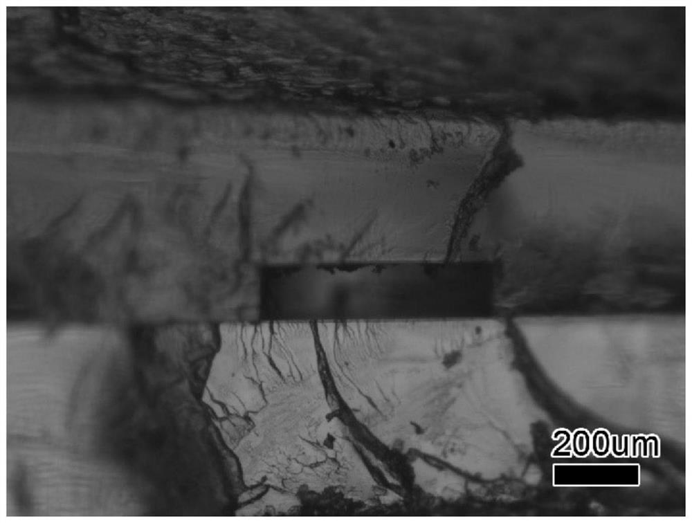
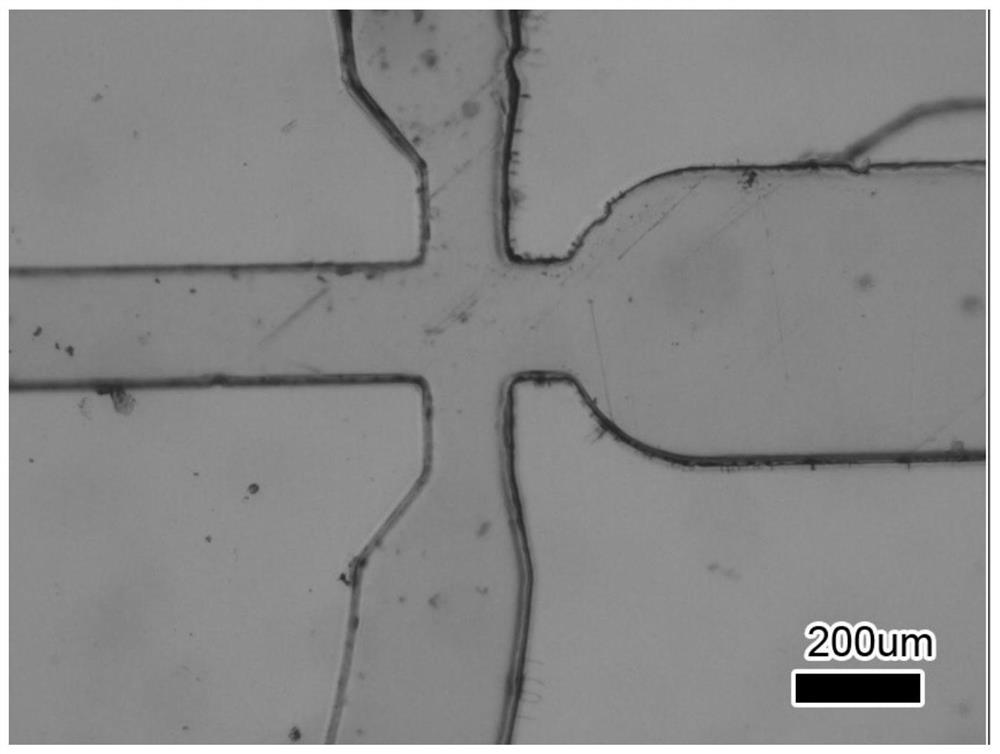
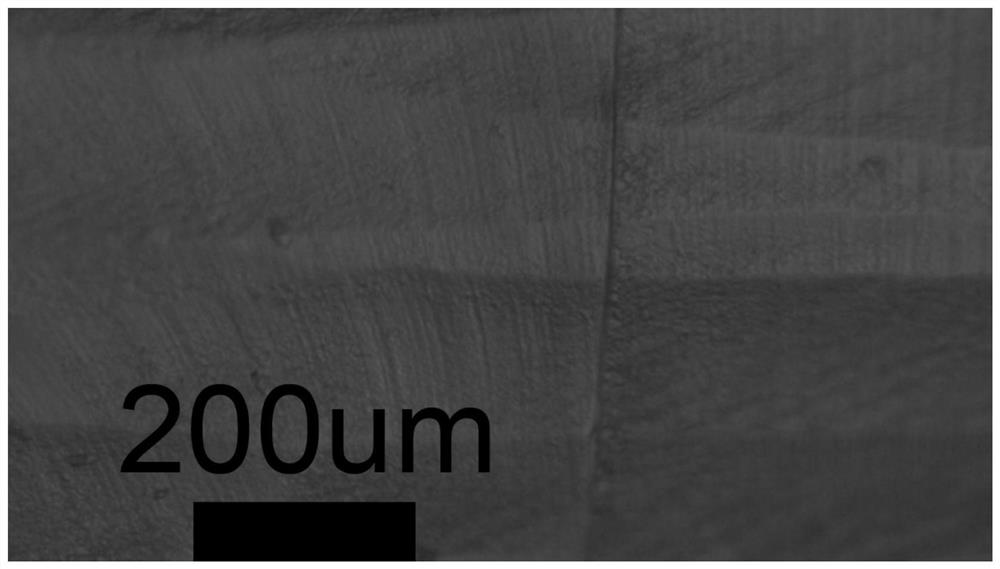
[0087] Embodiment 1 double-layer PMMA microfluidic chip sealing

[0088] The PMMA material chip with a complex microchannel structure is self-made, (patent application number 201611114889.1, Example 3) and the other is a PMMA cover sheet, both of which have a thickness of 1mm and a size of 8cm x 8cm. Dilute 0.5ml of PMMA glue chloroform into 2ml of hexane to form an adhesion promoter. Put the PMMA chip with complex microchannel structure and the PMMA cover sheet together, take 0.2ml of adhesion promoter and add it to the two PMMA sheets, put it into the tablet machine, the temperature of the pressure plate on the tablet machine is 50 degrees, and apply 0.5Mpa And keep it for 2 minutes, vacuum to remove excess liquid, and complete the sealing after 10 minutes. The micrographs of microchannel section, front surface and sealing surface after sealing are as follows: figure 1 , figure 2 and image 3 shown. The channel size measurement results show that the original height of ...

Embodiment 2

[0089] Embodiment 2 Double-layer PMMA microfluidic chip sealing

[0090] The PMMA material chip with a complex microchannel structure is self-made, and the other is a PMMA cover sheet. The thickness of both is 1mm, and the size is 8cm x 8cm. Dilute 0.9ml of PMMA glue chloroform into 2ml of hexane to form an adhesion promoter. Combine the PMMA chip with a complex microchannel structure and the PMMA cover sheet, add 0.2ml of adhesion promoter into the two PMMA sheets, put it into a tablet press, apply a pressure of 0.4Mpa at room temperature, and keep it for 10 minutes to complete the sealing. catch. The microchannel cross section after sealing, the front surface, the photomicrograph of the sealing surface, the channel size measurement results, the roughness test of the original PMMA microchannel and the microchannel after sealing are similar to those in Example 1. The depth of the cover slip embedded in the channel was less than 2 μm, which was less than 2% of the original ch...

Embodiment 3

[0091] Embodiment 3 double-layer PMMA microfluidic chip sealing

[0092] The PMMA material chip with a complex microchannel structure is self-made, and the other is a PMMA cover sheet. The thickness of both is 1mm, and the size is 8cm x 8cm. Dilute 0.9ml of PMMA glue chloroform into 2ml of cyclohexane to form an adhesion promoter. Combine the PMMA chip with complex microchannel structure and the PMMA cover sheet, take 0.2ml of adhesion promoter and add it to the two PMMA sheets, then put it into the tablet machine, apply 0.6Mpa pressure at room temperature, and keep it for 5 minutes Complete the seal. The microchannel cross section after sealing, the front surface, the photomicrograph of the sealing surface, the channel size measurement results, the roughness test of the original PMMA microchannel and the microchannel after sealing are similar to those in Example 1. The depth of the cover slip embedded in the channel was less than 2 μm, which was less than 2% of the original...


PUM

PropertyMeasurementUnit
depthaaaaaaaaaa
widthaaaaaaaaaa
widthaaaaaaaaaa

Abstract

The application discloses a method for sealing an acrylic-based microfluidic chip, which comprises the following steps: a) covering at least one layer of acrylic chip with a microchannel structure and a cover; b) adding an adhesion promoter to the covering within the structure; c) sealing under the conditions of 0-80°C and 0-1.0MPa to obtain the acrylic-based microfluidic chip; the microchannel structure in the sealed acrylic-based microfluidic chip is the same as the unsealed Compared with the microchannel structure, the height drop of the microchannel is less than 5 μm. The method can realize the non-destructive sealing of the acrylic material microfluidic chip with multi-layer and large-area complex structure. The acrylic glue is diluted with a solvent to reduce the corrosiveness of the glue, and realize the non-destructive sealing of multi-layer large-area microfluidic chips under low temperature and low pressure conditions.

Description

technical field [0001] The invention relates to a sealing method for an acrylic microfluidic chip, in particular to a sealing method for a non-destructive microchannel structure of an acrylic microfluidic chip with multiple layers, large area and complex structure. Background technique [0002] Microfluidic chip technology can realize flexible combination and functional integration of various technical units on a controllable platform by building a microchannel flow system on a chip with a size of several inches. In many fields, such as environmental testing, biopharmaceuticals, materials Synthesis, food safety and other aspects have potential application prospects, and have always been the focus of researchers from all over the world. [0003] At present, thermoplastic polymer materials have good light transmission, strong plasticity, and are suitable for mass production. They are excellent materials for preparing microfluidic chips, so they have attracted widespread attent...

Claims


Application Information

Patent Timeline
Patent Type & Authority Patents(China)
IPC IPC(8): B01L3/00
CPCB01L3/502707B01L2200/10B01L2300/0861B01L2300/0887B01L2300/12
Inventor 李春林刘中民魏迎旭
Owner DALIAN INST OF CHEM PHYSICS CHINESE ACAD OF SCI
Why Eureka
Try Eureka