
MEMS device and manufacturing method thereof

A manufacturing method and device technology, applied in the manufacture of microstructure devices, piezoelectric devices/electrostrictive devices, piezoelectric/electrostrictive/magnetostrictive devices, etc., to achieve good material compactness, ensure internal stress, and structure The effect of excellent performance

Active Publication Date: 2020-05-19
SEMICON MFG INT (SHANGHAI) CORP +1
View PDF6 Cites 4 Cited by
  • Summary
  • Abstract
  • Description
  • Claims
  • Application Information

AI Technical Summary

Problems solved by technology

[0004] In the prior art, the reliability of MEMS devices needs to be further improved

Method used


Image

  • MEMS device and manufacturing method thereof
  • MEMS device and manufacturing method thereof
  • MEMS device and manufacturing method thereof

Examples


Embodiment Construction

[0015] It can be seen from the background art that the performance of MEMS devices in the prior art needs to be improved.

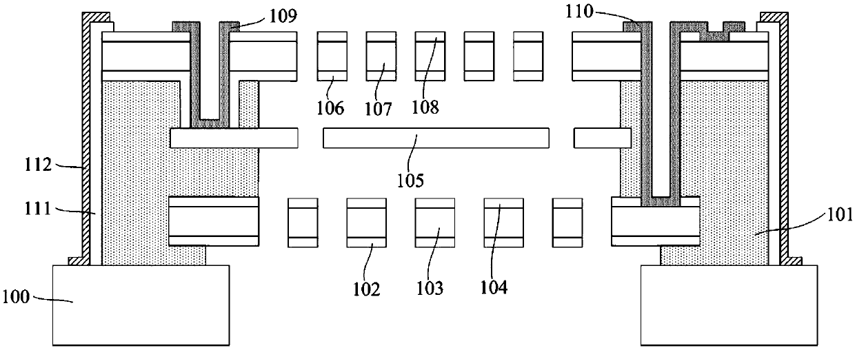
[0016] refer to figure 1 , figure 1 It is a schematic cross-sectional structure diagram of a double-back pole MEMS device, taking the double back pole MEMS device as a MEMS microphone as an example, and the MEMS device includes:

[0017] Substrate 100, the substrate 100 has a groove running through its thickness; a patterned first back plate located above the substrate 100, the first back plate includes a first lower plate 102, a first conductive electrode plate 103 and a first upper plate 104, the first back plate includes a first support area and a first vibration area, the first vibration area is located above the groove, and the first support area is located on the upper surface of the substrate 100 Above, and the first back plate of the first vibrating area has several openings through its thickness; the vibrating electrode located above the first ...


PUM


Abstract

The invention provides an MEMS device and a manufacturing method thereof. The MEMS device comprises a substrate with a back cavity, a vibration electrode located above the substrate, wherein the vibration electrode comprises support parts and a vibration part located between the support parts, an upper electrode plate located above the vibration electrode, a cantilever beam part positioned betweenthe supporting parts and the upper electrode plate and connecting the upper surfaces of the supporting parts and the lower surface of the upper electrode plate, and a sacrificial layer located on thesubstrate and further located on a part of the lower surface of the upper electrode plate, wherein a cavity is defined by the sacrificial layer, the upper electrode plate and the substrate, a back cavity, an opening and the cavity are communicated, the cantilever beam part and the vibration electrode are located in the cavity, and the material density of the cantilever beam part is larger than that of the sacrificial layer. According to the invention, the reliability of the MEMS device is improved in a manner of fixing the vibration electrode on the upper electrode plate by adopting the cantilever beam part.

Description

technical field [0001] The invention relates to the technical field of semiconductor manufacturing, in particular to a MEMS device and a manufacturing method thereof. Background technique [0002] Micro-Electro-Mechanical System (MEMS, Micro-Electro-Mechanical System) is based on microelectronics, micromechanics and material science, researching, designing, manufacturing, and micro-devices with specific functions. Micro-Electro-Mechanical Systems is a cutting-edge high technology with strategic significance for the cross-integration of multiple disciplines, and it will be one of the leading industries in the future. [0003] The advent and application of MEMS technology has made microphones smaller and smaller. MEMS microphones have many advantages, such as high signal-to-noise ratio, low power consumption, high sensitivity, the micro-package used is compatible with the placement process, reflow soldering has little impact on the performance of MEMS microphones, and excelle...

Claims


Application Information

Patent Timeline
IPC IPC(8): B81B3/00B81C1/00
CPCB81B3/0072B81C1/0015B81C1/00666
Inventor 王贤超
Owner SEMICON MFG INT (SHANGHAI) CORP
Learn More