Adjustable Fano resonance integrated device and preparation method thereof
An integrated device and resonance technology, which is applied in the field of tunable Fano resonance integrated devices and their preparation, can solve the problem that the resonance wavelength and slope of the Fano resonance spectral line cannot be adjusted, and the device cannot guarantee the stable generation of high-sharp Fano resonance spectral lines. and other problems, to achieve the effect of high application prospects
- Summary
- Abstract
- Description
- Claims
- Application Information
AI Technical Summary
Problems solved by technology
Method used
Image
Examples
Embodiment 1
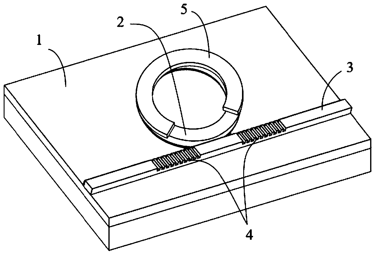
[0034] Such as figure 1 As shown, an adjustable Fano resonant integrated device includes a substrate 1, and also includes a microring waveguide 2 and a coupling straight waveguide 3 integrated on the substrate 1, and the top surface of the coupling straight waveguide 3 is provided The grating reflector 4 located at both ends of the coupling area and the micro heater 5 arranged above the micro-ring waveguide 2 .
[0035] In the specific implementation process, the Fabry-Perot resonator is formed by coupling the two grating reflectors 4 on the top surface of the straight waveguide 3. When the light wave enters from one end of the coupled straight waveguide 3, a part of the light is coupled into the microring resonator , oscillating to form a narrow Lorentz resonance line shape, the other part of the light oscillates in the Fabry-Perot resonator to form a wider resonance peak, and the two parts of light are coupled out to obtain the Fano resonance peak. The micro-heater 5 set ab...
Embodiment 2
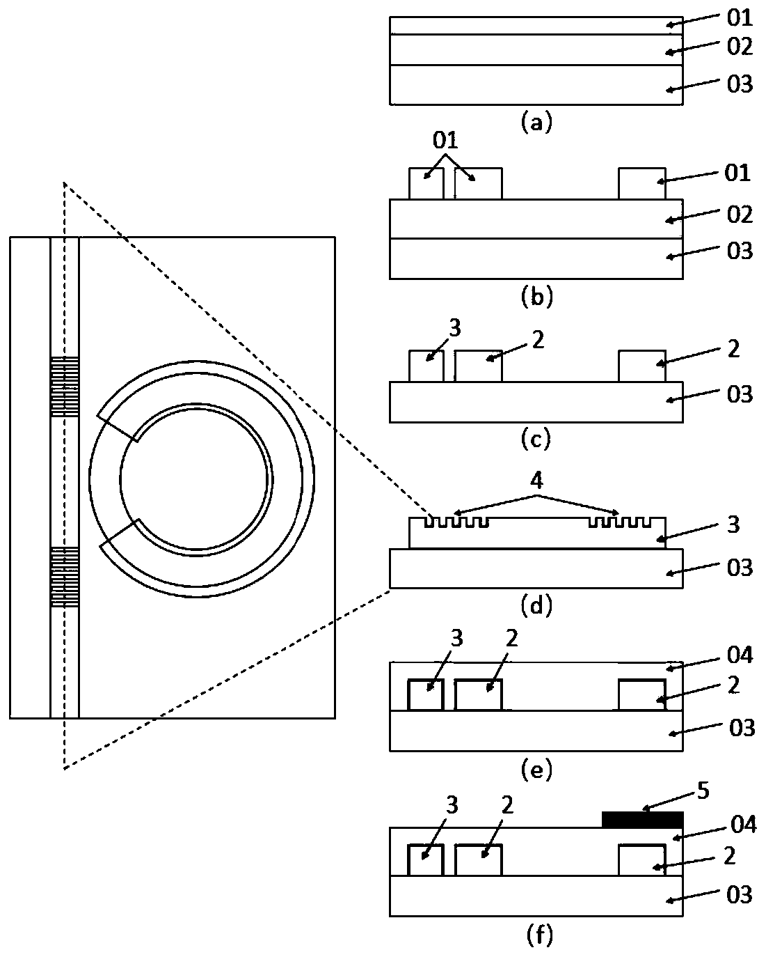
[0044] More specifically, on the basis of Example 1, such as figure 2 Shown in (a), (b), (c), (d), (e), and (f), a method for preparing an adjustable Fano resonant integrated device comprises the following steps:
[0045] S1: On the substrate 03, a deuterated silicon nitride layer 02 with a thickness of 560 nanometers is deposited by a chemical vapor phase method, and a positive photoresist 01 is spin-coated;
[0046] S2: Electron beam exposure is performed after spin-coating positive photoresist, and the micro-ring waveguide and coupled straight waveguide mask patterns are obtained after development;
[0047] S3: Etching out the microring waveguide 2 and the coupling straight waveguide 3 through a reactive ion etching process, and removing the photoresist;
[0048] S4: Spin-coat positive photoresist, perform electron beam exposure, and obtain a grating structure mask pattern after development, and shallowly etch a grating structure through a reactive ion etching process to ...
PUM
| Property | Measurement | Unit |
|---|---|---|
| Width | aaaaa | aaaaa |
| Width | aaaaa | aaaaa |
| Length | aaaaa | aaaaa |
Abstract
Description
Claims
Application Information
 - R&D
- Intellectual Property
- Life Sciences
- Materials
- Tech Scout
- Unparalleled Data Quality
- Higher Quality Content
- 60% Fewer Hallucinations
Browse by: Latest US Patents, China's latest patents, Technical Efficacy Thesaurus, Application Domain, Technology Topic, Popular Technical Reports.
© 2025 PatSnap. All rights reserved.Legal|Privacy policy|Modern Slavery Act Transparency Statement|Sitemap|About US| Contact US: help@patsnap.com


