Special graph avoiding method and device for optimizing manufacturability of integrated circuit

An integrated circuit, manufacturable technology, applied in special data processing applications, electrical digital data processing, instruments, etc., to achieve the effect of optimizing and improving manufacturability

Active Publication Date: 2020-05-19
PHYTIUM TECH CO LTD
View PDF8 Cites 2 Cited by
  • Summary
  • Abstract
  • Description
  • Claims
  • Application Information

AI Technical Summary

Problems solved by technology

The solution idea of ​​the present invention is to avoid the adjacency of these standard cells in certain specific directions in the back-end design of the integrated circuit. Since the process documents provided by the process manufacturer are used to solve the design rule problem of the bottom layer area of ​​the bottom standard cell, the present invention Will increase fabrication success rates on bottom standard cell area and bottom two metal layers by extending process house documentation

Method used


Image

  • Special graph avoiding method and device for optimizing manufacturability of integrated circuit
  • Special graph avoiding method and device for optimizing manufacturability of integrated circuit
  • Special graph avoiding method and device for optimizing manufacturability of integrated circuit

Examples


Embodiment 1

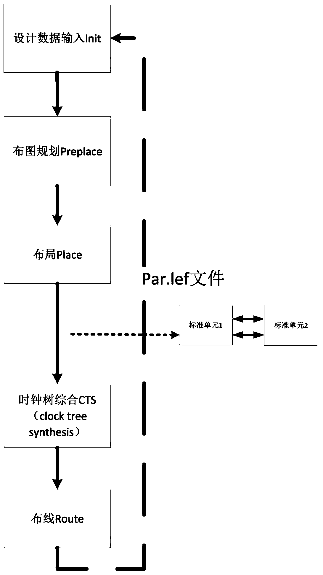
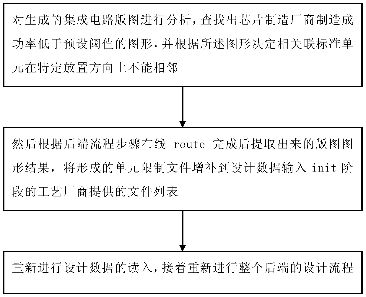
[0026] Such as figure 2 As shown, according to a special graphic circumvention method for optimizing the manufacturability of an integrated circuit according to an embodiment of the present invention, the integrated circuit back-end process includes design data input Init, layout planning Preplace, layout Place, clock tree synthesis CTS (clock tree synthesis) and five basic steps of wiring Route. After the above steps are completed, analyze the generated integrated circuit layout, find out the graphics whose manufacturing success rate is lower than the preset threshold by the chip manufacturer, and decide according to the graphics Associated standard cells cannot be adjacent to each other in a specific placement direction; then, according to the layout graphics results extracted after the routing route is completed in the back-end process steps, a cell restriction file is formed, and the formed cell restriction file is added to the design data input process in the init stage ...

Embodiment 2

[0035] This embodiment describes the present invention from the perspective of hardware, a special graphics avoidance device for optimizing the manufacturability of integrated circuits, a back-end design module, and the back-end process of the integrated circuit is executed through the back-end design module, and the process includes design data Input the five basic steps of Init, layout planning Preplace, layout Place, clock tree synthesis CTS (clock tree synthesis) and routing Route, including the analysis module, which is executed after the above steps are completed, and the generated integrated circuit layout is analyzed. Analyze and find out the graphics whose manufacturing success rate is lower than the preset threshold by the chip manufacturer, and determine that the associated standard units cannot be adjacent in a specific placement direction according to the graphics; the execution module, the execution module is wired according to the back-end process steps After the...


PUM


Abstract

The invention discloses a special graph avoiding method for optimizing manufacturability of an integrated circuit. The back-end process of the integrated circuit comprises five basic steps of design data input, layout planning, layout, clock tree synthesis and wiring, after the steps are completed, a generated integrated circuit layout is analyzed, a graph with the manufacturing success rate of achip manufacturer lower than a preset threshold value is found out, and it is determined that associated standard units cannot be adjacent in the specific placement direction according to the graph; and then, according to a layout graphic result extracted after the wiring of the back-end process step is completed, the formed unit limiting file is supplemented into a file list provided by a processmanufacturer in the init stage of inputting the design data, the design data is read in again, and then, the whole back-end design process is carried out again. According to the method, files related to process manufacturing provided by process manufacturers and EDA tool manufacturers do not need to be modified, and new file formats of the EDA tool manufacturers do not need to be supplemented.

Description

technical field [0001] The invention relates to the field of IC design, in particular to a special pattern avoidance method and device for optimizing the manufacturability of integrated circuits. Background technique [0002] With the rapid development of semiconductor manufacturing technology, in order to achieve faster computing speed, larger storage capacity and realize more functions, semiconductor chips are developing towards higher integration. The higher the integration of semiconductor chips, the more complicated the manufacturing process is. The current advanced integrated circuit manufacturing process generally contains hundreds of process steps. Therefore, a problem in one of the steps will cause problems in the entire semiconductor chip. , which shows that the performance of the integrated circuit fails to meet the design requirements, and in serious cases may lead to the failure of the entire chip. [0003] Therefore, it is particularly important to find out th...

Claims


Application Information

Patent Timeline
Patent Type & Authority Applications(China)
IPC IPC(8): G06F30/392G06F30/398G06F119/18
Inventor 王飞马卓田金峰宋佳利郭御风张明张少华丁军锋
Owner PHYTIUM TECH CO LTD
Why Eureka
Try Eureka