A method for preparing a hollow structure on the surface and inside of a transparent material

A technology of transparent materials and hollow structures, applied in the field of femtosecond laser micro-nano processing, can solve the problems of high environmental requirements and low processing efficiency, and achieve the effect of wide application prospects

Active Publication Date: 2021-07-27
JILIN UNIV
View PDF8 Cites 1 Cited by
  • Summary
  • Abstract
  • Description
  • Claims
  • Application Information

AI Technical Summary

Problems solved by technology

The method of the present invention can realize high-efficiency and high-precision processing of various common transparent materials in a vacuum-free environment, and solves the problems of relatively high environmental requirements and low processing efficiency in the prior art

Method used


Image

  • A method for preparing a hollow structure on the surface and inside of a transparent material
  • A method for preparing a hollow structure on the surface and inside of a transparent material
  • A method for preparing a hollow structure on the surface and inside of a transparent material

Examples


Embodiment 1

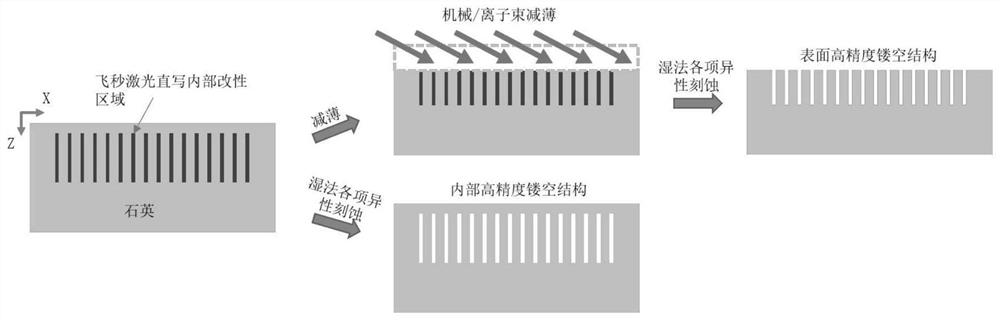
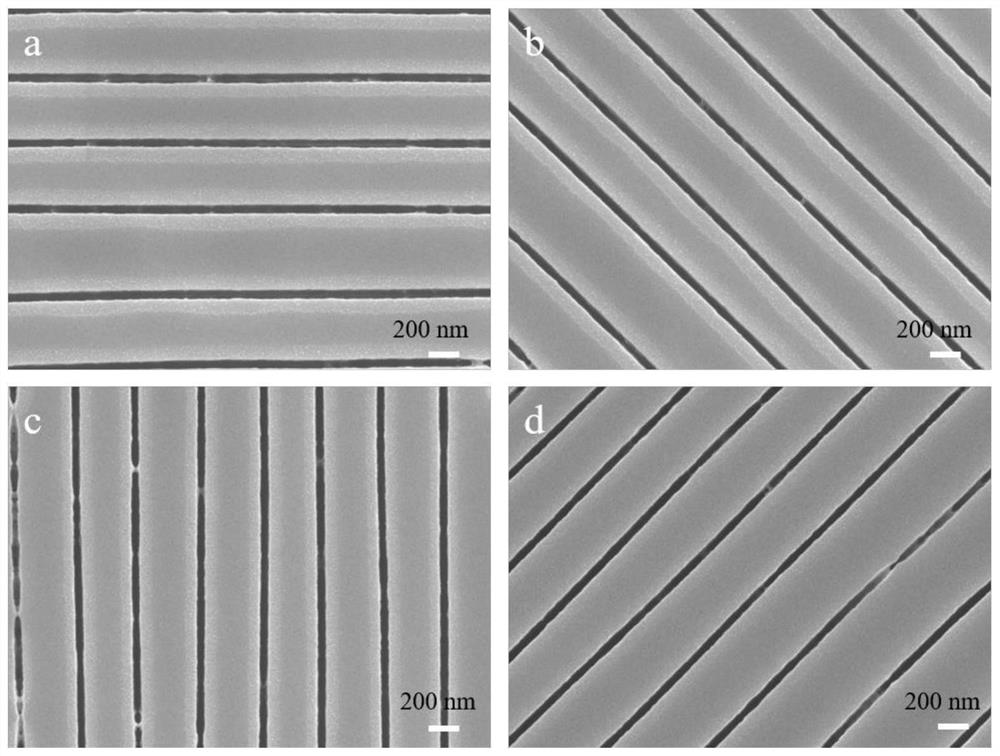
[0030] Quartz surface processing high-precision nanowire array structure

[0031] A femtosecond laser is used to write a uniform line structure inside the quartz, and then the sample is polished to the vicinity of the processing area by mechanical polishing, and then an anisotropic etching is performed by a wet etching process, so as to realize a uniform nanowire array structure on the quartz surface.

[0032] A method for preparing an ultra-high-precision structure on the surface of a transparent hard and brittle material, the specific steps are as follows:

[0033] (1), sample preparation and leveling;

[0034] First, a bulk fused silica sample with a thickness of 500 μm was cut into 20x20mm by a glass knife 2 , placed in acetone and alcohol test tubes for ultrasonic treatment for 20 minutes, and finally placed in a beaker filled with deionized water for 10 minutes, and dried with nitrogen. Then use double-sided adhesive tape to attach the quartz sample to a glass slide, a...

Embodiment 2

[0043] Nanowire Array Structure in 45-degree Direction on YAG Crystal Surface

[0044] A femtosecond laser is used to write a uniform nanometer-precision modified structure inside the YAG crystal, and an ion beam thinner is used to quantitatively thin the surface of the YAG crystal. Finally, an anisotropic etching of the YAG is performed using a wet etching process.

[0045] (1) Leveling of the sample stage:

[0046] Same as example 1.

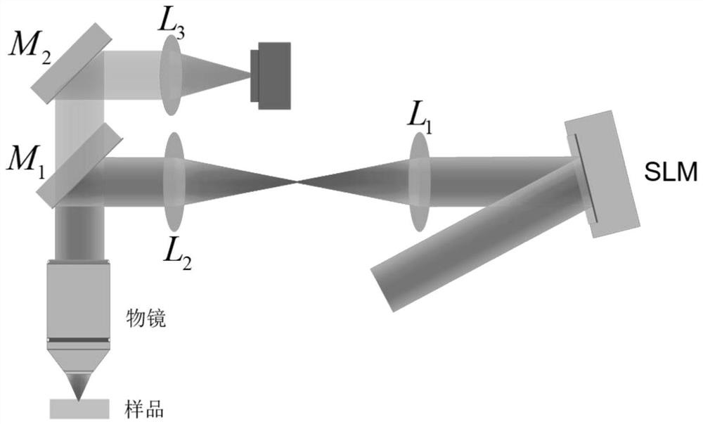
[0047] (2) Writing of uniform nanostructures inside YAG

[0048] Same as Example 1, the only difference is that different spherical aberration correction holograms are loaded on the spatial light modulator and the single pulse energy used. The single pulse energy used here is 247nJ, and the internal depth is 30um.

[0049] (3) Focused ion beam thinning

[0050] Paste the prepared YAG sample evenly on the aluminum column of the ion beam thinning instrument with quick-drying adhesive, put the aluminum column into the ion beam thinning instru...


PUM

PropertyMeasurementUnit
thicknessaaaaaaaaaa
thicknessaaaaaaaaaa

Abstract

The invention discloses a method for preparing a hollow structure on the surface and inside of a transparent material, which belongs to the technical field of femtosecond laser micro-nano processing. The invention uses a femtosecond laser direct writing method to write inside a transparent material through precise control of polarization and processing power. Directly write the modified area with an accuracy of hundreds of nanometers, then use mechanical / ion beam thinning to thin the surface of the transparent material to the position of the processed area (surface processing), and finally use wet etching to etch the material, Finally, the preparation of a hollow structure with a precision of hundreds of nanometers and an arbitrary patterned structure was realized. The method of the invention can realize high-efficiency and high-precision processing of various common transparent materials in a vacuum-free environment, and solves the problems of relatively high environmental requirements and low processing efficiency in the prior art.

Description

technical field [0001] The invention belongs to the technical field of femtosecond laser micro-nano processing, and specifically relates to using a femtosecond laser to directly write a uniform line structure with a precision of 100 nanometers inside a transparent material. Through subsequent polishing and wet etching processes, the surface and interior ultrahigh Processing accuracy and the preparation of hollow structures with arbitrary depth-to-diameter ratios. Background technique [0002] With the continuous advancement of science and technology, people have higher and higher requirements for integration and miniaturization. Compared with large-scale devices with the same function, devices prepared using micro-nano structures not only have low energy consumption, high efficiency, and high sensitivity. Advantages, and at the same time, due to its small size, it is convenient for multi-functional integration. The same is true for optics. In recent years, the preparation ...

Claims


Application Information

Patent Timeline
Patent Type & Authority Patents(China)
IPC IPC(8): B23K26/362B23K26/0622B23K26/352B23K26/70B08B3/02B08B3/08B24B1/00
CPCB08B3/02B08B3/08B23K26/362B24B1/00B23K26/0622B23K26/352B23K26/702
Inventor 孙洪波樊华陈岐岱
Owner JILIN UNIV
Why Eureka
Try Eureka