
Single-pixel infrared and visible light dual-band sensor and array

A visible light, dual-band technology, applied in the direction of electrical components, electrical solid-state devices, semiconductor devices, etc., can solve the problems of unable to collect light signals, etc., and achieve the advantages of focal plane, material growth and device manufacturing process with simple and high precision Effect

Inactive Publication Date: 2020-05-22
UNIV OF ELECTRONICS SCI & TECH OF CHINA
View PDF4 Cites 0 Cited by
  • Summary
  • Abstract
  • Description
  • Claims
  • Application Information

AI Technical Summary

Problems solved by technology

At the same time, when the dual-band sensor in the prior art collects infrared and visible light, it can only collect light from different angles of view, and cannot collect signals from light incident on the same field of view.

Method used


Image

  • Single-pixel infrared and visible light dual-band sensor and array
  • Single-pixel infrared and visible light dual-band sensor and array
  • Single-pixel infrared and visible light dual-band sensor and array

Examples


Embodiment

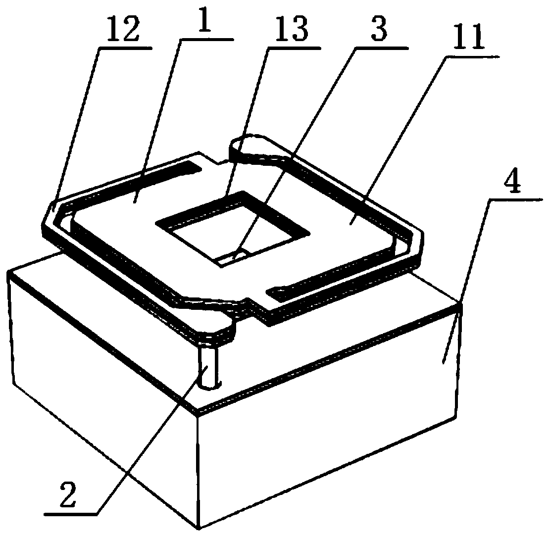
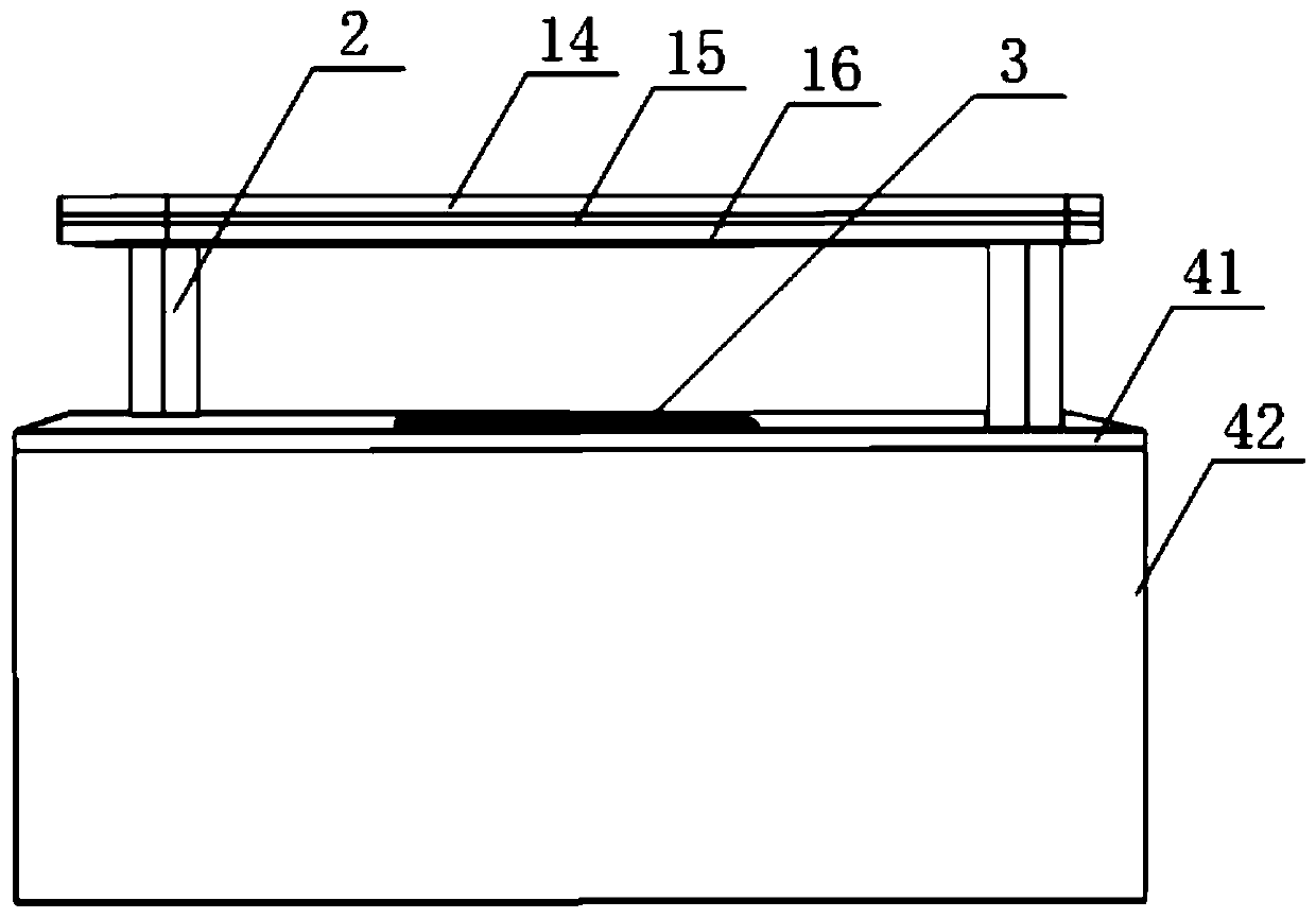
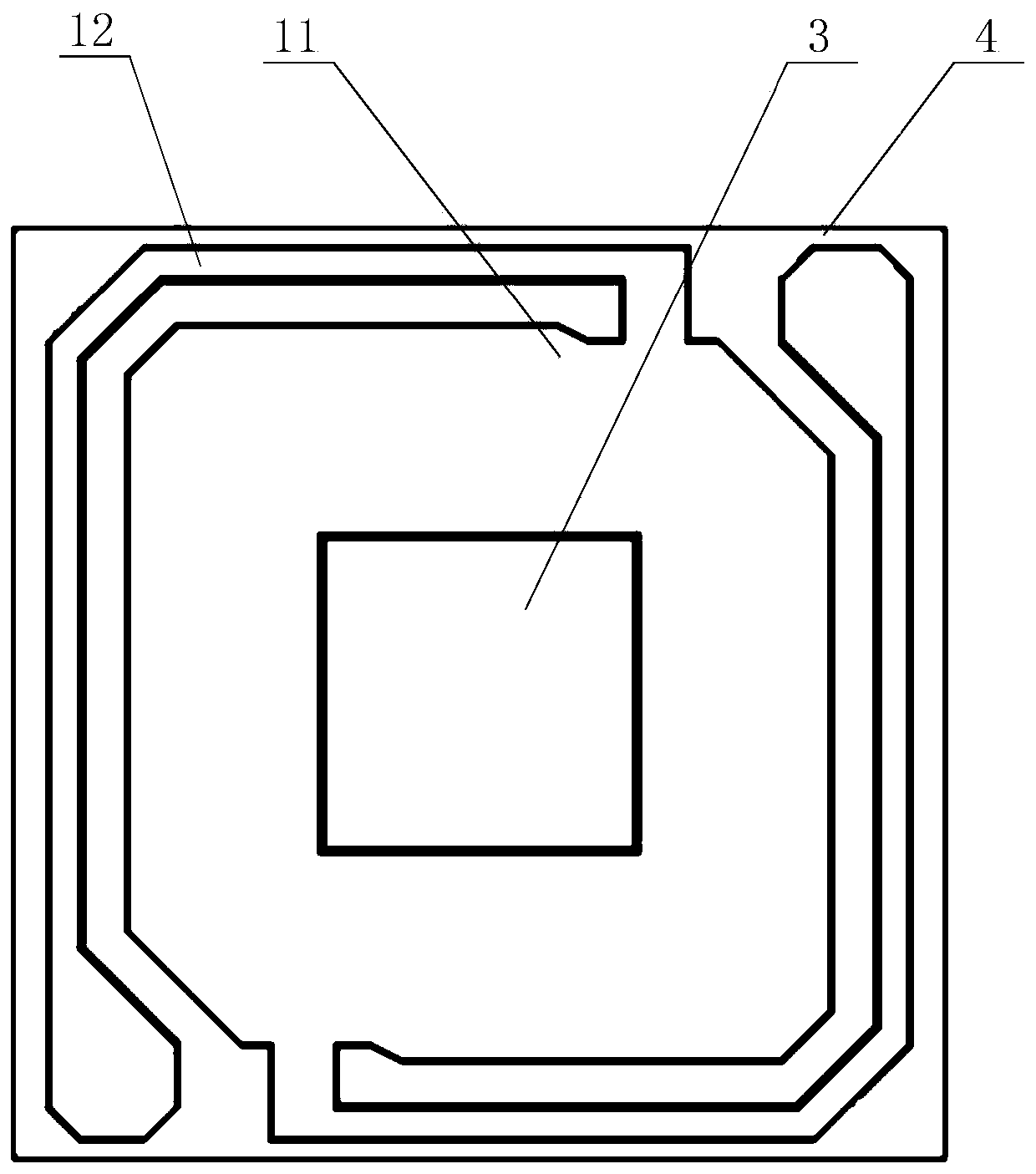
[0032] Such as Figure 1~3 As shown, a single-pixel infrared and visible light dual-band sensor of the present invention includes an upper photosensitive component 1, a bridge column 2, a visible light photosensitive component 3 and a silicon substrate 4; the upper layer photosensitive component 1 is installed through the bridge column 2 Above the silicon substrate 4, and the visible light photosensitive element 3 is arranged on the upper surface of the silicon substrate 4; the upper photosensitive element 1 is provided with a light-transmitting through hole 13, and the visible light photosensitive element 3 Located directly below the light-transmitting through hole 13 .

[0033] When this embodiment is implemented, in view of the defects in the prior art, the upper photosensitive component is sensitive to the light in the infrared band, and the visible light photosensitive component is sensitive to the light in the visible light band; when the light incident at the same viewi...


PUM

PropertyMeasurementUnit
thicknessaaaaaaaaaa
thicknessaaaaaaaaaa
thicknessaaaaaaaaaa

Abstract

The invention discloses a single-pixel infrared and visible light dual-waveband sensor. The sensor comprises an upper photosensitive component, a bridge column, a visible light photosensitive component and a silicon substrate, wherein the upper layer photosensitive assembly is installed above the silicon substrate through the bridge column, and the visible light photosensitive assembly is arrangedon the upper surface of the silicon substrate; a light-transmitting through hole is formed in the upper-layer photosensitive assembly, and the visible light photosensitive assembly is located under the light-transmitting through hole. The invention further discloses a single-pixel infrared and visible light dual-band sensor array. According to the single-pixel infrared and visible light double-waveband sensor and the array, visible light and infrared double wavebands can be detected at the same time in a single pixel, and target information is richer. Meanwhile, material growth and device manufacturing processes are simple, and focal planarization of the device is facilitated.

Description

technical field [0001] The invention relates to the technical field of infrared and visible light detection and imaging, in particular to a single-pixel infrared and visible light dual-band sensor and array. Background technique [0002] Infrared detection technology has special advantages: invisible infrared radiation, good confidentiality; good environmental adaptability; passive receiving system, strong anti-interference ability; small size, light weight, low power consumption; can reveal camouflaged targets ; The resolution is better than microwave, so it is widely used in infrared night vision, infrared detection, infrared guidance and other fields. At present, relatively mature photon detectors have been applied to the fields of communication and medicine. Uncooled infrared focal plane array technology has become the most mainstream direction of infrared detection technology. This technology allows us to obtain infrared detectors with high sensitivity at room temperat...

Claims


Application Information

Patent Timeline
Patent Type & Authority Applications(China)
IPC IPC(8): H01L27/146G01J1/42
CPCH01L27/14603H01L27/14605G01J1/42
Inventor 吕坚邹灵乐张逸鲁竞原阙隆成周云
Owner UNIV OF ELECTRONICS SCI & TECH OF CHINA
Learn More