Delay phase-locked loop circuit, clock signal synchronization method and semiconductor memory
A clock signal and delay signal technology, which is applied in the field of semiconductor integrated circuits, can solve the problems of excessive power consumption of the delay chain, and achieve the effect of ensuring reliability and accuracy and reducing consumption
- Summary
- Abstract
- Description
- Claims
- Application Information
AI Technical Summary
Problems solved by technology
Method used
Image

Examples
Embodiment Construction
[0054] In the following, only some exemplary embodiments are briefly described. As those skilled in the art would realize, the described embodiments may be modified in various different ways, all without departing from the spirit or scope of the present invention. Accordingly, the drawings and descriptions are to be regarded as illustrative in nature and not restrictive.
[0055] In a first aspect, an embodiment of the present invention provides a delay phase-locked loop circuit.
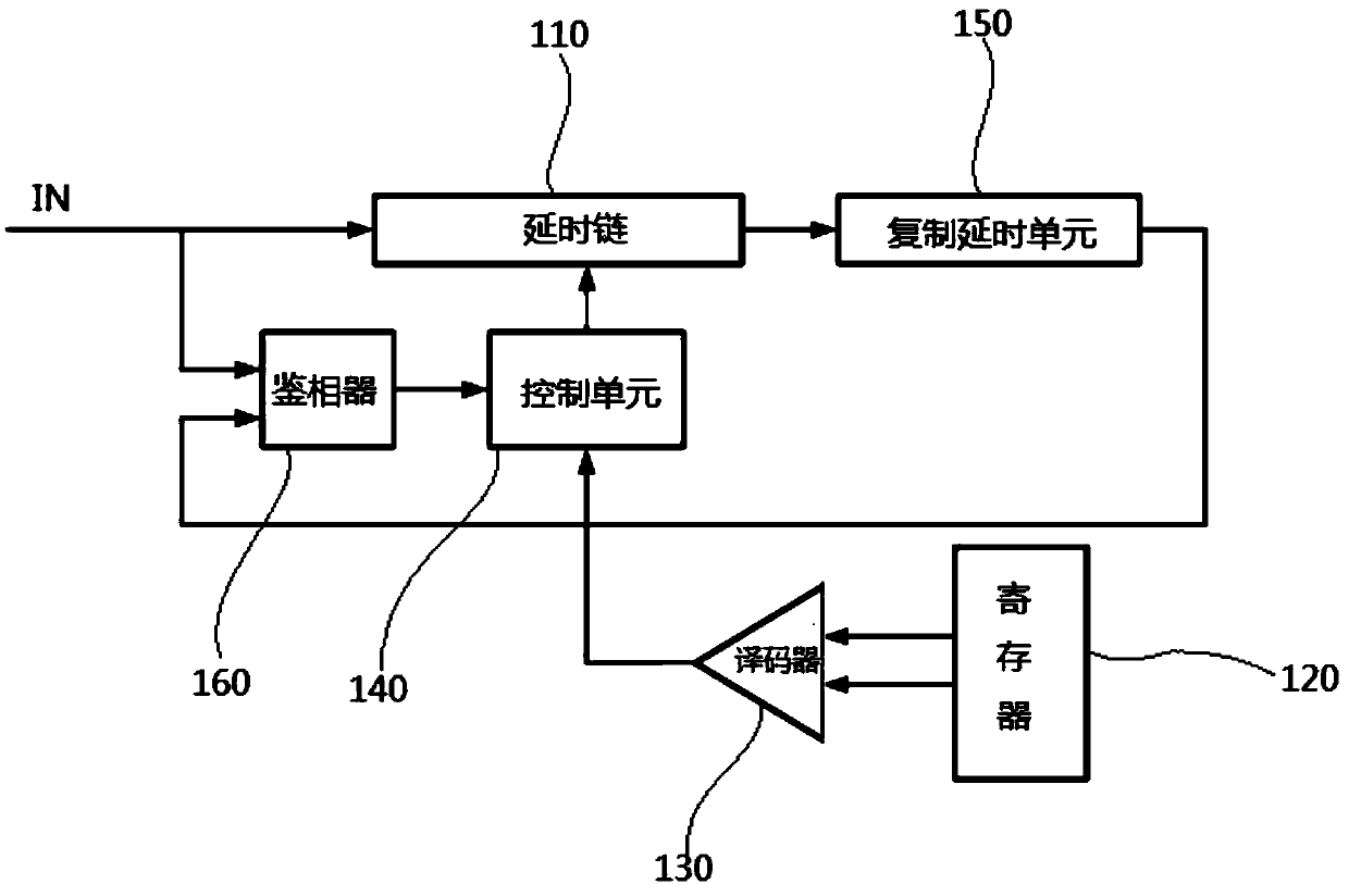
[0056] see figure 1 As shown, the delay phase locked loop circuit may include a delay chain 110 , a decoder 130 , a control unit 140 , a replica delay unit 150 and a phase detector 160 .
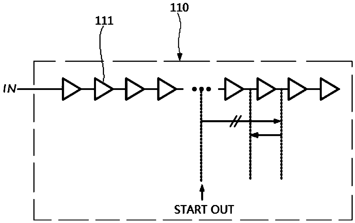
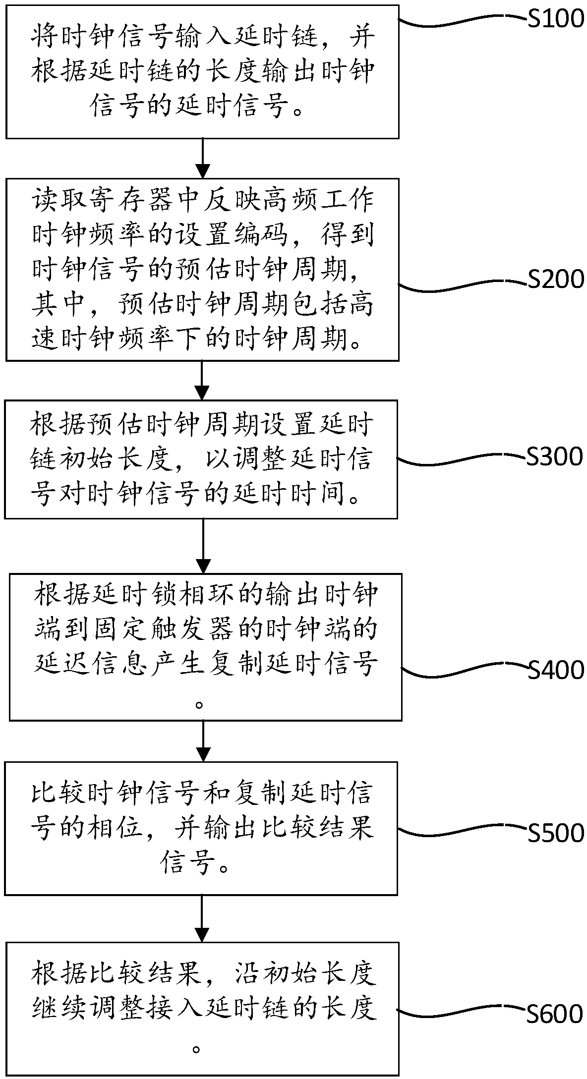
[0057] The delay chain 110 can be used to input a clock signal, and output a delayed signal of the clock signal according to the length of the delay chain 110 . Because the memory chip will switch the clock frequency during the working process. For example, when synchronizing the clock signal, when the DDR4 cl...
PUM
 Abstract
Description
Claims
Application Information
 - R&D
- Intellectual Property
- Life Sciences
- Materials
- Tech Scout
- Unparalleled Data Quality
- Higher Quality Content
- 60% Fewer Hallucinations
Browse by: Latest US Patents, China's latest patents, Technical Efficacy Thesaurus, Application Domain, Technology Topic, Popular Technical Reports.
© 2025 PatSnap. All rights reserved.Legal|Privacy policy|Modern Slavery Act Transparency Statement|Sitemap|About US| Contact US: help@patsnap.com