Modulation method of asymmetric ferroelectric tunneling junction multi-value storage unit
A technology of multi-value storage and modulation method, which is applied in the direction of electrical components, information storage, static memory, etc., to achieve the effect of increasing unit storage capacity, fast speed, and increasing storage density
- Summary
- Abstract
- Description
- Claims
- Application Information
AI Technical Summary
Problems solved by technology
Method used
Image
Examples
preparation example Construction
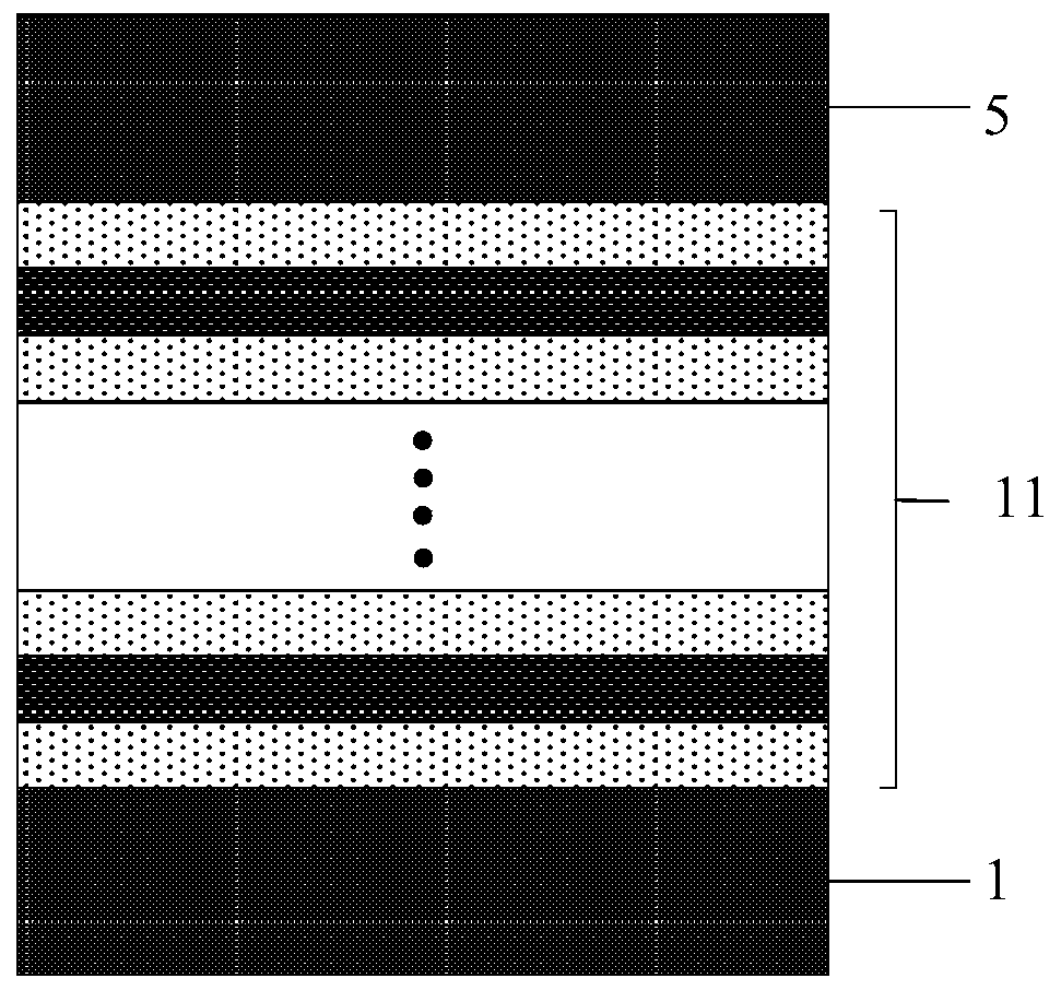
[0075] The present invention provides a method for preparing the above-mentioned multi-valued storage unit of the asymmetric ferroelectric tunnel junction, the multi-valued storage unit includes the above-mentioned
[0076] The method includes the following steps:
[0077] Step 1: providing a substrate, and forming a first electrode layer 1 on the upper surface of the substrate;
[0078] Step 2: Form an asymmetric ferroelectric functional layer array 11 on the upper surface of the first electrode layer 1, which includes: N ferroelectric functional layers parallel to the first plane direction, two adjacent ferroelectric functional layers separated by an insulating layer;
[0079] Step 3: forming a second electrode layer 5 on the upper surface of the Nth ferroelectric functional layer;
[0080] Step 4: crystallizing the ferroelectric functional layer, so that the material of the ferroelectric functional layer exhibits ferroelectric properties;
[0081] In the present inventio...
Embodiment
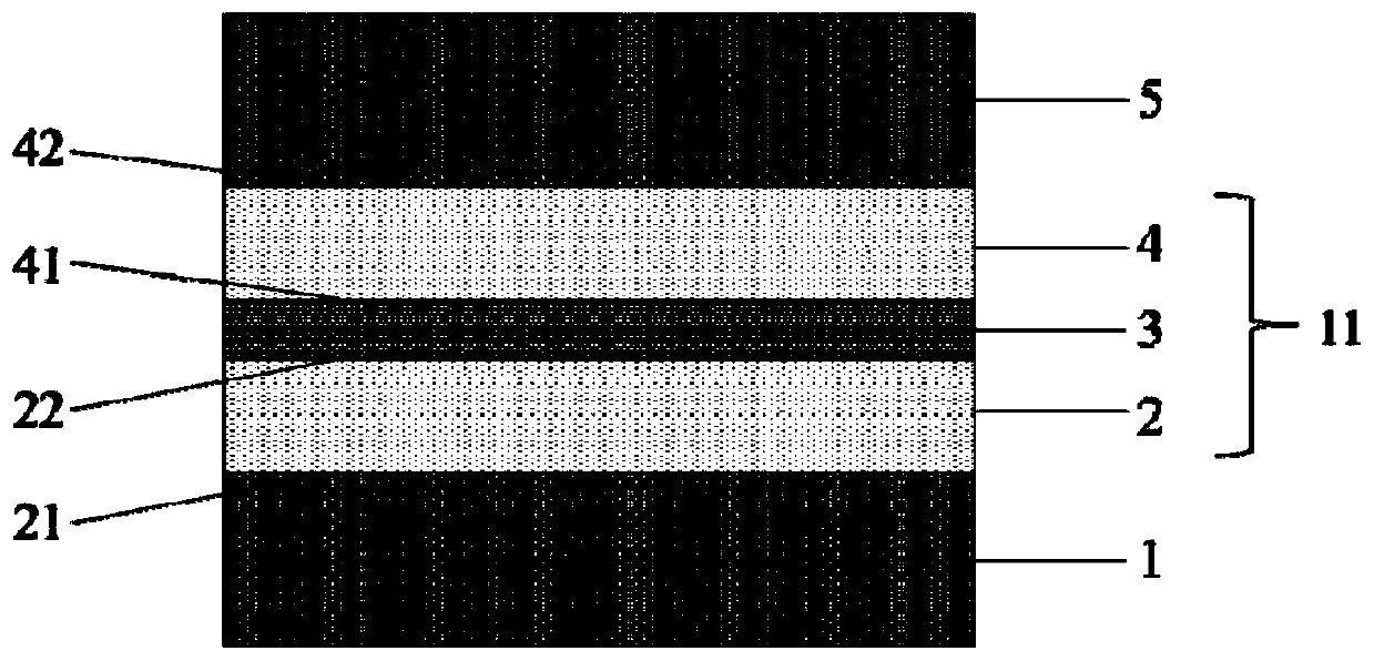
[0106] This embodiment provides a Hf-based 0.5 Zr 0.5 o 2 (hereinafter abbreviated as HZO) ferroelectric thin film and Al 2 o 3 The multi-value storage unit of the asymmetric ferroelectric tunnel junction of the insulating layer, its structure schematic diagram is as follows figure 1 As shown, it mainly includes a first electrode layer 1 , a first ferroelectric functional layer 2 , an insulating layer 3 , a second ferroelectric functional layer 4 , and a second electrode layer 5 from bottom to top. Specific steps are as follows:
[0107] (1) Preparation of the first electrode layer 1
[0108] Step 1: Preparation of the first electrode layer 1: TiN is selected as the lower electrode 1 in the embodiment, and a layer of the lower electrode 1 is grown on a single crystal silicon substrate with SiO2 polished on one side by magnetron sputtering.
[0109] Step 1-1: Substrate cleaning: first use acetone to clean in an ultrasonic environment for 10 minutes, then use alcohol to cl...
PUM
| Property | Measurement | Unit |
|---|---|---|
| Thickness | aaaaa | aaaaa |
| Thickness | aaaaa | aaaaa |
| Thickness | aaaaa | aaaaa |
Abstract
Description
Claims
Application Information


