
Preparation method of Si-based substrate heterogeneous integrated graphene

A technology of graphene and graphene layers, applied in the direction of graphene, nano-carbon, etc., can solve the problems of incompatibility of substrate materials with common processes, difficulty in controlling the size of graphene films, etc., and achieve the effect of expanding the scope of application

Pending Publication Date: 2020-06-02
SHANGHAI INST OF MICROSYSTEM & INFORMATION TECH CHINESE ACAD OF SCI
View PDF5 Cites 4 Cited by
  • Summary
  • Abstract
  • Description
  • Claims
  • Application Information

AI Technical Summary

Problems solved by technology

It is used to solve the problems of difficulty in controlling the size of existing graphene films and the incompatibility of substrate materials with common processes

Method used


Image

  • Preparation method of Si-based substrate heterogeneous integrated graphene
  • Preparation method of Si-based substrate heterogeneous integrated graphene
  • Preparation method of Si-based substrate heterogeneous integrated graphene

Examples


Embodiment 1

[0078] Such as Figure 1 to Figure 7 As shown, the present embodiment provides a method for fabricating a Si-based substrate heterogeneously integrated graphene film, comprising steps:

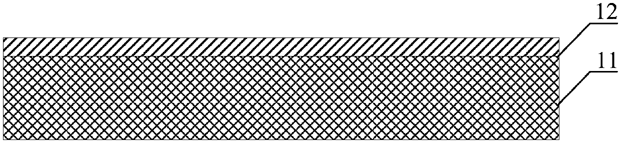
[0079] Such as figure 1 As shown, step 1) is performed to provide a Si-based substrate 11, and a dielectric layer 12 is formed on the upper surface of the Si-based substrate.

[0080] Optionally, the material of the dielectric layer 12 includes but not limited to silicon oxide, aluminum oxide, and silicon nitride.

[0081] As an example, silicon oxide is selected as the dielectric layer in step 1).

[0082] Optionally, the thickness of the dielectric layer 12 is greater than 0 nm and less than or equal to 1 μm.

[0083] Optionally, the growth method of the dielectric layer 12 includes but not limited to thermal oxidation method and vapor phase deposition method.

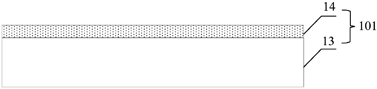
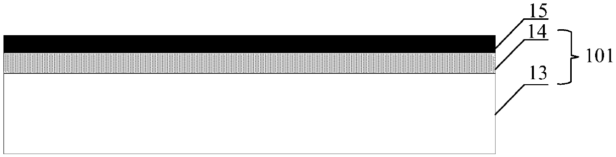
[0084] Such as figure 2 As shown, step 2) is performed to provide a composite structure 101, the composite structure 101 incl...

Embodiment 2

[0113] Such as Figure 8 ~ Figure 14 As shown, the present embodiment provides a method for fabricating a Si-based substrate heterogeneously integrated graphene film, comprising steps:

[0114] Such as Figure 8 As shown, step 1) is performed to provide a Si-based substrate 21, and a dielectric layer 22 is formed on the upper surface of the Si-based substrate.

[0115] Optionally, the material of the dielectric layer 22 includes but not limited to silicon oxide, aluminum oxide, and silicon nitride.

[0116] Optionally, the thickness of the dielectric layer 22 is greater than 0 nm and less than or equal to 1 μm.

[0117] Optionally, the growth method of the dielectric layer 22 includes but not limited to thermal oxidation method and vapor phase deposition method.

[0118] Such as Figure 9 As shown, step 2) is performed to provide a composite structure 201, the composite structure 201 includes a sacrificial substrate 23 and a metal layer 24 covering the surface of the sacri...

Embodiment 3

[0144] Such as Figure 15 ~ Figure 20 As shown, the present embodiment provides a method for fabricating a Si-based substrate heterogeneously integrated graphene film, comprising steps:

[0145] Such as Figure 15 As shown, step 1) is performed to provide a Si-based substrate 31, and a dielectric layer 32 is formed on the upper surface of the Si-based substrate.

[0146] Optionally, the material of the dielectric layer 32 includes but not limited to silicon oxide, aluminum oxide, and silicon nitride.

[0147] Optionally, the thickness of the dielectric layer 32 is greater than 0 nm and less than or equal to 1 μm.

[0148] Optionally, step 1) further includes planarizing the Si-based substrate dielectric layer 32 .

[0149] As an example, the Si-based substrate dielectric layer 32 is planarized so that the surface of the dielectric layer is atomically flat.

[0150] Optionally, the planarization method includes but not limited to chemical mechanical polishing and ion beam p...


PUM

PropertyMeasurementUnit
thicknessaaaaaaaaaa
thicknessaaaaaaaaaa
electron mobilityaaaaaaaaaa

Abstract

The invention relates to a preparation method of Si-based substrate heterogeneous integrated graphene. The method comprises the following steps: providing a Si-based substrate, and forming a dielectric layer on the upper surface of the Si-based substrate; providing a composite structure, wherein the composite structure comprises a sacrificial substrate and a metal layer covering the upper surfaceof the sacrificial substrate; depositing a graphene film on the upper surface of the composite structure to form a graphene layer covering the metal layer; bonding the side, covered with the dielectric layer, of the Si-based substrate with the side, covered with the graphene film, of the composite structure; and etching the metal layer by adopting an etching process to realize separation of the sacrificial substrate, so that the graphene film is transferred to the Si-based substrate. According to the method, a graphene film is transferred to a Si-based substrate, so that the problem of wafer-level integration of the graphene film and the Si-based substrate is solved, and support is provided for application of graphene in the field of microelectronic devices.

Description

technical field [0001] The invention belongs to the field of preparation of functional materials, in particular to a method for preparing Si-based substrate heterogeneously integrated graphene. Background technique [0002] Graphene is a single-layer planar compact two-dimensional honeycomb lattice of carbon atoms. It is a single-layer two-dimensional crystal composed of carbon atoms arranged in sp2 hybrid orbitals. It is the basic building block of graphite materials in all other dimensions. It can be packed into zero-dimensional fullerenes, rolled into one-dimensional nanotubes or stacked into three-dimensional graphite. The structure of graphene is very stable, the carbon-carbon bond spacing is only When subjected to an external force, graphene will bend and deform to release the stress, and the carbon atoms do not need to be rearranged to maintain a stable structure. This structure also makes graphene have excellent thermal conductivity, and electrons in graphene will...

Claims


Application Information

Patent Timeline
Patent Type & Authority Applications(China)
IPC IPC(8): C01B32/186
CPCC01B32/186
Inventor 欧欣伊艾伦林家杰张师斌于庆凯谢晓明
Owner SHANGHAI INST OF MICROSYSTEM & INFORMATION TECH CHINESE ACAD OF SCI
Learn More