

Double-time-step photomultiplier
A photomultiplier and device technology, applied in the field of photoelectric detection, can solve the problems of signal retention, reduced system space utilization, and long signal processing time.
- Summary
- Abstract
- Description
- Claims
- Application Information
AI Technical Summary
Problems solved by technology
Method used
Image

Examples
Embodiment Construction
[0030] The following will clearly and completely describe the technical solutions in the embodiments of the present invention with reference to the drawings in the embodiments of the present invention.
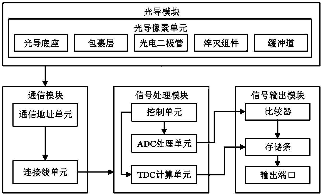
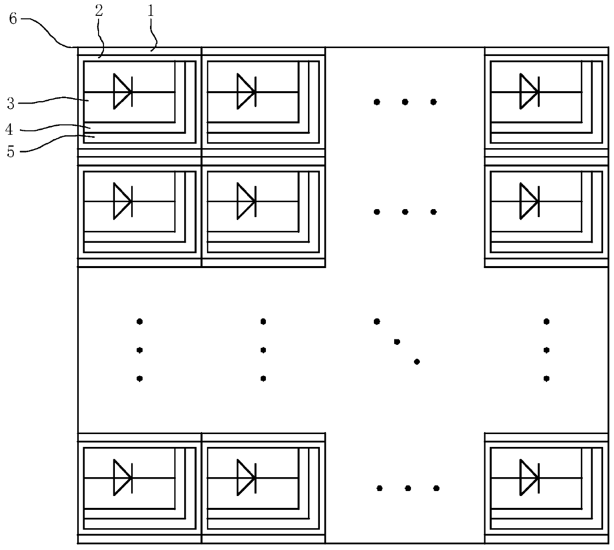
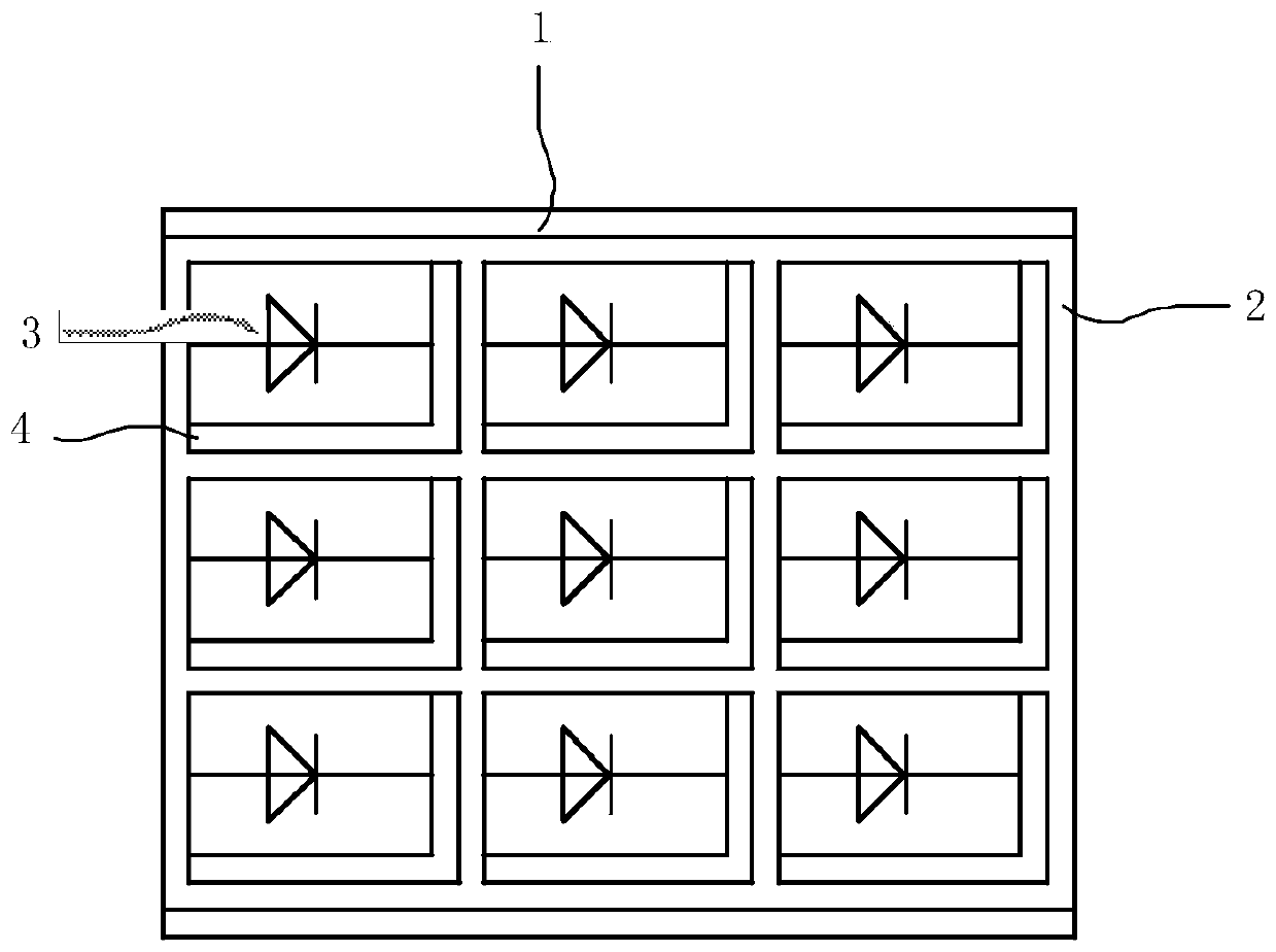
[0031] Such as Figure 1-4 As shown, one embodiment of the present invention discloses a dual-time-step photomultiplier device, including a photoconductive module for detecting photons, a communication module, a signal processing module, and a signal output module; the photoconductive module includes a plurality of photoconductive pixel units 6, A plurality of photoconductive pixel units 6 are distributed in an array to form a photoconductive array; the photoconductive pixel unit 6 includes a photoconductive base 1, a wrapping layer 2, a photodiode 3, a quenching assembly 4, and a buffer channel 5; the wrapping layer 2 is located on the photoconductive base 1, and the photodiode 3 is located in the wrapping layer 2, the quenching component 4 surrounds the outside of the photod...
PUM
 Abstract
Description
Claims
Application Information