Shield gate trench MOSFET

A technology of shielding gates and trenches, applied in the direction of electrical components, circuits, semiconductor devices, etc., can solve problems such as drop

A technology of shielding gates and trenches, applied in the direction of electrical components, circuits, semiconductor devices, etc., can solve problems such as drop

CN111223930APending Publication Date: 2020-06-02SHENZHEN SANRISE TECH CO LTD

Image

  • Shield gate trench MOSFET
  • Shield gate trench MOSFET
  • Shield gate trench MOSFET

Examples


Embodiment Construction

[0084] Shielded gate trench MOSFET according to the first embodiment of the present invention:

[0085] The shielded gate trench MOSFET according to the first embodiment of the present invention includes: a primary cell region and a peripheral region, and the peripheral region is located on the periphery of the primary cell region.

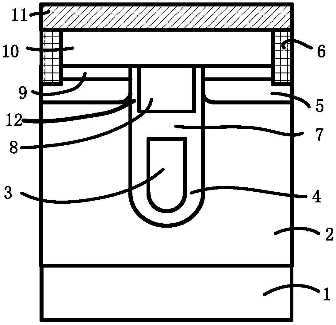
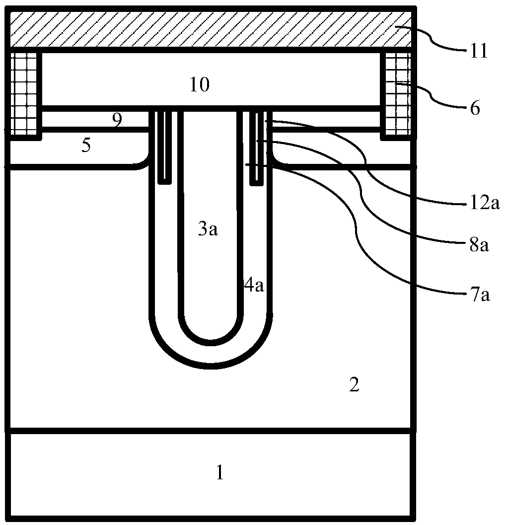
[0086] The device unit structure of the shielded gate trench MOSFET is formed in the primary cell region. For the device unit structure of the first embodiment of the present invention, please refer to figure 1 As shown, each of the device unit structures includes:

[0087] The first gate structure is formed in the first trench, including the first polysilicon shielding field plate 3 and the first polysilicon gate 8 stacked together; the first trench is formed in the first conductivity type doped In the impurity first epitaxial layer 2, a first shielding dielectric layer 4 is isolated between the first polysilicon shielding field plate 3 and the ...


PUM


Abstract

The invention discloses a shield gate trench metal oxide semiconductor field effect transistor (MOSFET). The structure comprises a primitive cell region and a peripheral region, a device unit structure of a shield gate trench MOSFET is formed in the primitive cell region, a trench MOS capacitor used for reducing nonlinearity of output capacitance of the shield gate trench MOSFET is formed in the peripheral region, and the trench MOS capacitor comprises a second gate structure which is formed in a second trench and comprises a second polycrystalline silicon shield field plate, wherein the second trench is formed in a first epitaxial layer doped with the first conductivity type, and a second shielding dielectric layer is isolated between the second polycrystalline silicon shielding field plate and the first epitaxial layer, the source region is not formed on the surface of the first epitaxial layer covered on the side surface of the second trench, and the first epitaxial layer on the side surface of the second trench and the first epitaxial layer of the primitive cell region form the drift region of the whole device; the drain region of the whole device is formed at the bottom of thefirst epitaxial layer; and the top of the second polycrystalline silicon shielding field plate is connected to the source electrode through a contact hole. According to the invention, the minimum value of the output capacitance can be improved, and the nonlinearity of the output capacitance is improved.

Description

technical field [0001] The invention relates to a semiconductor integrated circuit, in particular to a shielded gate trench (SGT) MOSFET. Background technique [0002] like figure 1 Shown is the structural schematic diagram of the device unit structure of the existing first shielded gate trench MOSFET; the existing first shielded gate trench MOSFET is formed by parallel connection of multiple device unit structures in the original cell region, each The device unit structure includes: [0003] The first gate structure is formed in the first trench, including the first polysilicon shielding field plate 3 and the first polysilicon gate 8 stacked together; the first trench is formed in the first conductivity type doped In the impurity first epitaxial layer 2, a first shielding dielectric layer 4 is isolated between the first polysilicon shielding field plate 3 and the first epitaxial layer 2, and the first polysilicon gate 8 A first gate dielectric layer 12 is isolated from t...

Claims


Application Information

Patent Timeline
02 Jun 2020
Publication
CN111223930A
IPC
H01L29/78; H01L29/423; H01L29/40; H01L29/06
CPC
H01L29/7813; H01L29/402; H01L29/4236; H01L29/0684
Inventors
่’‹ๅฎน; ่‚–่ƒœๅฎ‰