Organic compound and preparation method thereof, and application in OLED
A technology of organic compounds and compounds, applied in organic chemistry, chemical instruments and methods, semiconductor/solid-state device manufacturing, etc., can solve problems such as complex manufacturing process and affecting the angular distribution of OLED radiation spectrum
- Summary
- Abstract
- Description
- Claims
- Application Information
AI Technical Summary
Problems solved by technology
Method used
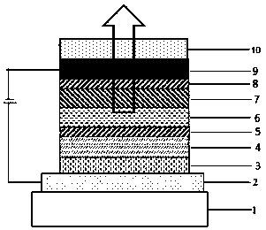
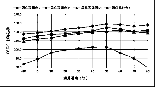
Image

Examples
Embodiment 1
[0078] Embodiment 1: the synthesis of compound 2:
[0079]
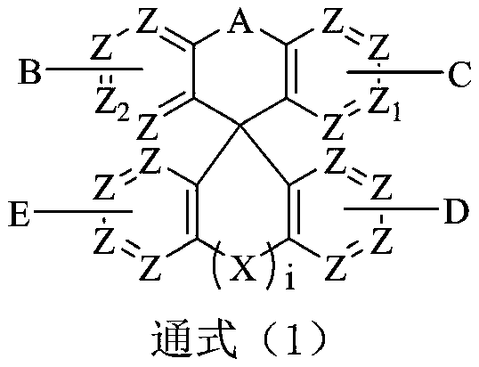
[0080] In a 250ml three-neck flask, under the protection of nitrogen, add 0.01mol raw material A1, 0.012mol raw material B1, 150ml toluene and stir to mix, then add 1×10 -4 molPd (pph 3 ) 4 , heated to 105 ° C, reflux reaction for 24 hours, sampling point plate, showing no bromide remaining, the reaction is complete; naturally cooled to room temperature, filtered, and the filtrate was subjected to vacuum rotary evaporation (-0.09MPa, 85 ° C), passed through neutral silica gel column, the target product was obtained with a HPLC purity of 99.17% and a yield of 79.8%. Elemental analysis structure (molecular formula C 51 h 30 N 2 o 2 ): theoretical value: C, 87.16; H, 4.30; N, 3.99; 0, 4.55; test value: C, 87.14; HPLC-MS: The molecular weight of the material is 702.23, and the measured molecular weight is 702.27.
[0081] The following compounds were prepared in the same manner as in Example 1 (the raw materia...
PUM
| Property | Measurement | Unit |
|---|---|---|
| Thickness | aaaaa | aaaaa |
| Thickness | aaaaa | aaaaa |
Abstract
Description
Claims
Application Information
 - R&D
- Intellectual Property
- Life Sciences
- Materials
- Tech Scout
- Unparalleled Data Quality
- Higher Quality Content
- 60% Fewer Hallucinations
Browse by: Latest US Patents, China's latest patents, Technical Efficacy Thesaurus, Application Domain, Technology Topic, Popular Technical Reports.
© 2025 PatSnap. All rights reserved.Legal|Privacy policy|Modern Slavery Act Transparency Statement|Sitemap|About US| Contact US: help@patsnap.com