
GaN-based LED epitaxial structure, preparation method thereof and light emitting diode

An epitaxial structure and electrode technology, which is applied in the direction of electrical components, circuits, semiconductor devices, etc., can solve the problems of AlInN and AlGaInN material growth difficulties, reduce hole injection barriers, etc., achieve high barrier electron leakage and reduce barrier barriers , Improve the effect of luminous efficiency

Inactive Publication Date: 2020-06-12
GUANGDONG INST OF SEMICON IND TECH
View PDF5 Cites 2 Cited by
  • Summary
  • Abstract
  • Description
  • Claims
  • Application Information

AI Technical Summary

Problems solved by technology

In order to reduce the influence of the polarization effect on the height of the electron blocking barrier, it has been reported that the use of a polarity-matched AlInN or AlGaInN layer can theoretically reduce the polarization charge between the electron blocking layer and the quantum barrier, thereby increasing the effective electron blocking potential. barrier, but the actual growth of AlInN and AlGaInN materials is more difficult
At present, there is no effective means to prevent the leakage of electrons in the active region to the p-doped region of the light-emitting diode, and at the same time reduce the blocking barrier of hole injection, so as to achieve the improvement of electron blocking efficiency and hole injection efficiency.

Method used


Image

  • GaN-based LED epitaxial structure, preparation method thereof and light emitting diode
  • GaN-based LED epitaxial structure, preparation method thereof and light emitting diode
  • GaN-based LED epitaxial structure, preparation method thereof and light emitting diode

Examples


no. 1 example

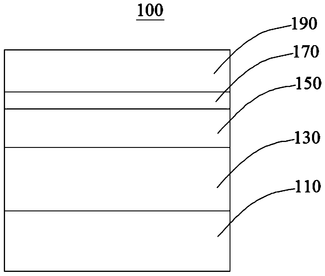
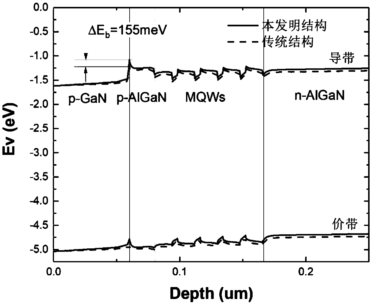
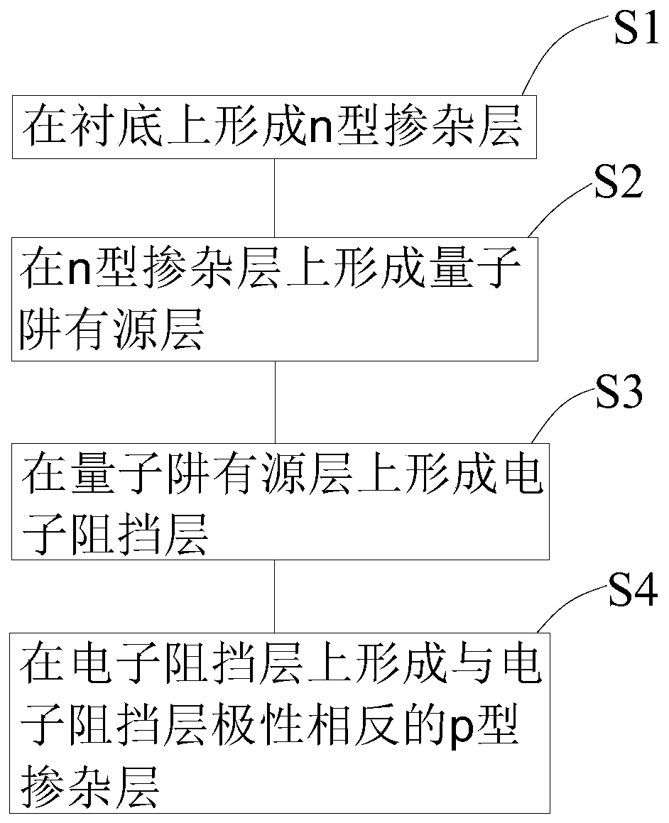
[0048] see in conjunction figure 1 and figure 2 , the present embodiment provides a GaN-based LED epitaxial structure 100, which is suitable for the light emitting diode 200, and can improve the electron blocking efficiency and hole injection efficiency, thereby improving the luminous efficiency of the light emitting diode 200.

[0049] The GaN-based LED epitaxial structure 100 provided in this embodiment includes a substrate 110, an n-type doped layer 130, a quantum well active layer 150, an electron blocking layer 170, and a p-type doped layer 190 arranged sequentially from bottom to top, The n-type doped layer 130 is formed on the substrate 110, the quantum well active layer 150 is formed on the n-type doped layer 130, the electron blocking layer 170 is formed on the quantum well active layer 150, and the p-type doped layer 190 is formed On the electron blocking layer 170 , the polarity of the p-type doped layer 190 is opposite to that of the electron blocking layer 170 ....

no. 2 example

[0073] see Figure 4 , this embodiment provides a light emitting diode 200, including a P electrode 210, an N electrode 230 and a GaN-based LED epitaxial structure 100, wherein the basic structure and principle of the GaN-based LED epitaxial structure 100 and the technical effects produced are the same as those of the first embodiment Similarly, for brief description, for parts not mentioned in this embodiment, reference may be made to the corresponding content in the first embodiment.

[0074] The light emitting diode 200 provided in this embodiment includes a P electrode 210, an N electrode 230, and a GaN-based LED epitaxial structure 100. The GaN-based LED epitaxial structure 100 includes a substrate 110, an n-type doped layer 130 formed on the substrate 110, formed The quantum well active layer 150 on the n-type doped layer 130, the electron blocking layer 170 formed on the quantum well active layer 150, and the p-type doped layer 190 formed on the electron blocking layer ...


PUM


Abstract

The invention provides a GaN-based LED epitaxial structure, a preparation method thereof and a light emitting diode, relates to the technical field of semiconductors, the GaN-based LED epitaxial structure comprises a substrate, an n-type doped layer, a quantum well active layer, an electron blocking layer and a p-type doped layer which are sequentially arranged from bottom to top, wherein the n-type doped layer is formed on the substrate, the quantum well active layer is formed on the n-type doped layer, the electron blocking layer is formed on the quantum well active layer, the p-type doped layer is formed on the electron blocking layer, and the polarity of the p-type doped layer is opposite to that of the electron blocking layer. High-density net polarization negative charges exist at the interface of the polarity of the p-type doping layer and the electron blocking layer; therefore, the conduction band energy level of the electron blocking layer is induced to be raised to be higher,a higher barrier is generated to block electron leakage, meanwhile, the blocking barrier of hole injection is reduced, the electron blocking efficiency and the hole injection efficiency are improved,and thus the light emitting efficiency of the light emitting diode is improved.

Description

technical field [0001] The invention relates to the technical field of semiconductors, in particular to a GaN-based LED epitaxial structure, a preparation method thereof, and a light-emitting diode. Background technique [0002] GaN-based light-emitting diodes (LEDs) usually face the problems of reduced luminous efficiency and increased heat generation under high current. Leakage of electrons from the active region of the quantum well structure is considered to be one of the main causes of efficiency drop. In order to prevent electron leakage, an electron blocking layer, such as an AlGaN layer, is usually added between the active region and the p-type region. The electron blocking layer has a higher conduction band energy level than the quantum barrier, and thus can block electrons from leaking from the active region to the p-type region. However, due to the influence of polarized charges at the interface between the electron blocking layer and the quantum barrier, the ene...

Claims


Application Information

Patent Timeline
Patent Type & Authority Applications(China)
IPC IPC(8): H01L33/14H01L33/32H01L33/00
CPCH01L33/0075H01L33/14H01L33/145H01L33/325
Inventor 李成果曾巧玉张康姜南赵维陈志涛
Owner GUANGDONG INST OF SEMICON IND TECH
Learn More