Electrically-driven optical antenna light source and manufacturing method thereof

A technology of optical antenna and manufacturing method, which is applied to circuits, electrical components, semiconductor devices, etc., can solve the problems of reducing the space size of the light source, the response speed of the light source being limited, the radiation attenuation time, etc.

Pending Publication Date: 2020-06-16
WUHAN UNIV
View PDF0 Cites 3 Cited by
  • Summary
  • Abstract
  • Description
  • Claims
  • Application Information

AI Technical Summary

Problems solved by technology

After ignoring the frequency limitation of the circuit's own capacitance-resistance loop, the response speed of this type of light source is only limited by the time for electrons to tunnel through the potential barrier and the time for the radiation decay of the local field energy itself
Therefore, in theory, the upper limit of the operating frequency of this type of light source is in the range of 10-100THz
At the same time, due to the sub-wavelength scale characteristics of the optical antenna itself, this will greatly reduce the spatial size of the light source

Method used


Image

  • Electrically-driven optical antenna light source and manufacturing method thereof
  • Electrically-driven optical antenna light source and manufacturing method thereof
  • Electrically-driven optical antenna light source and manufacturing method thereof

Examples


Embodiment 1

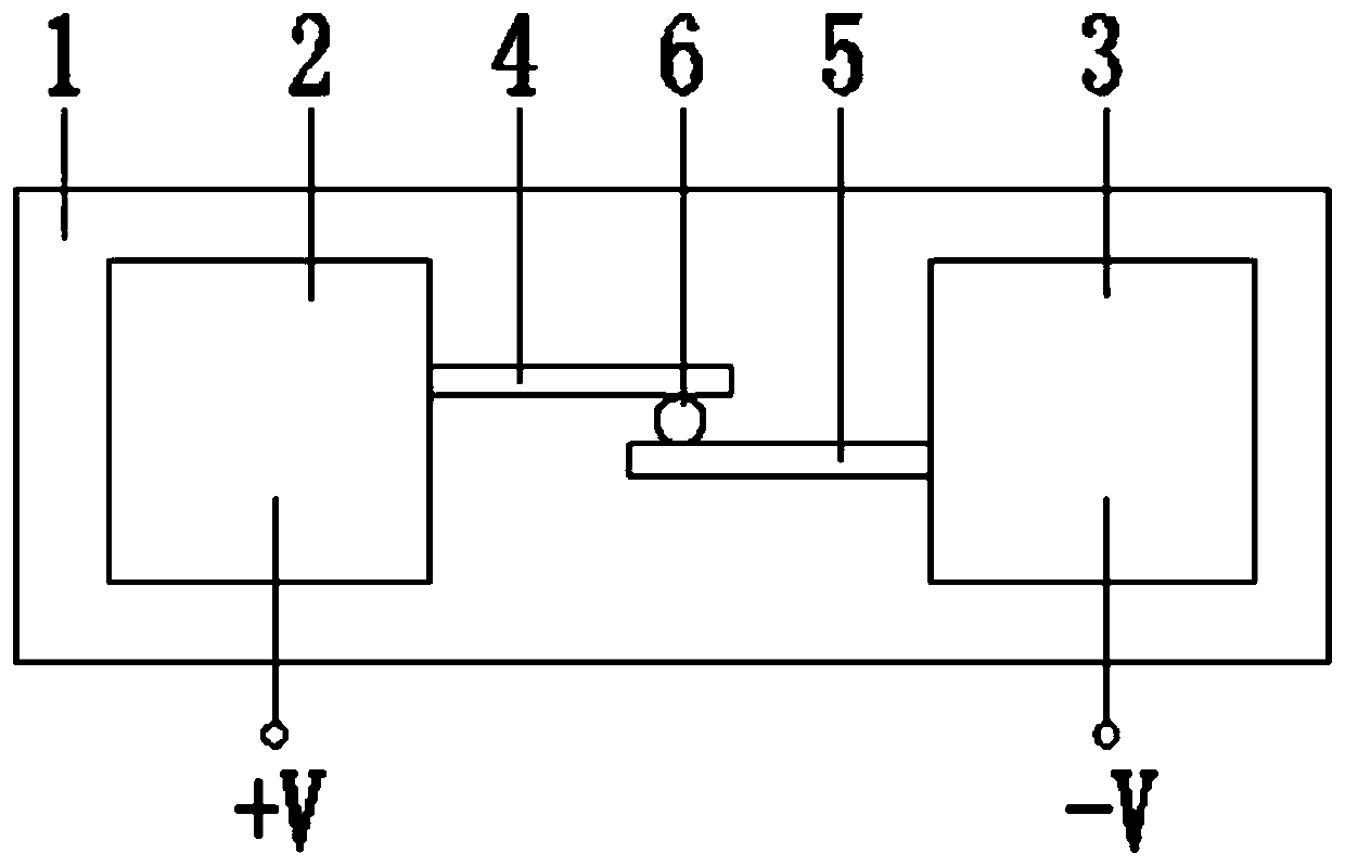
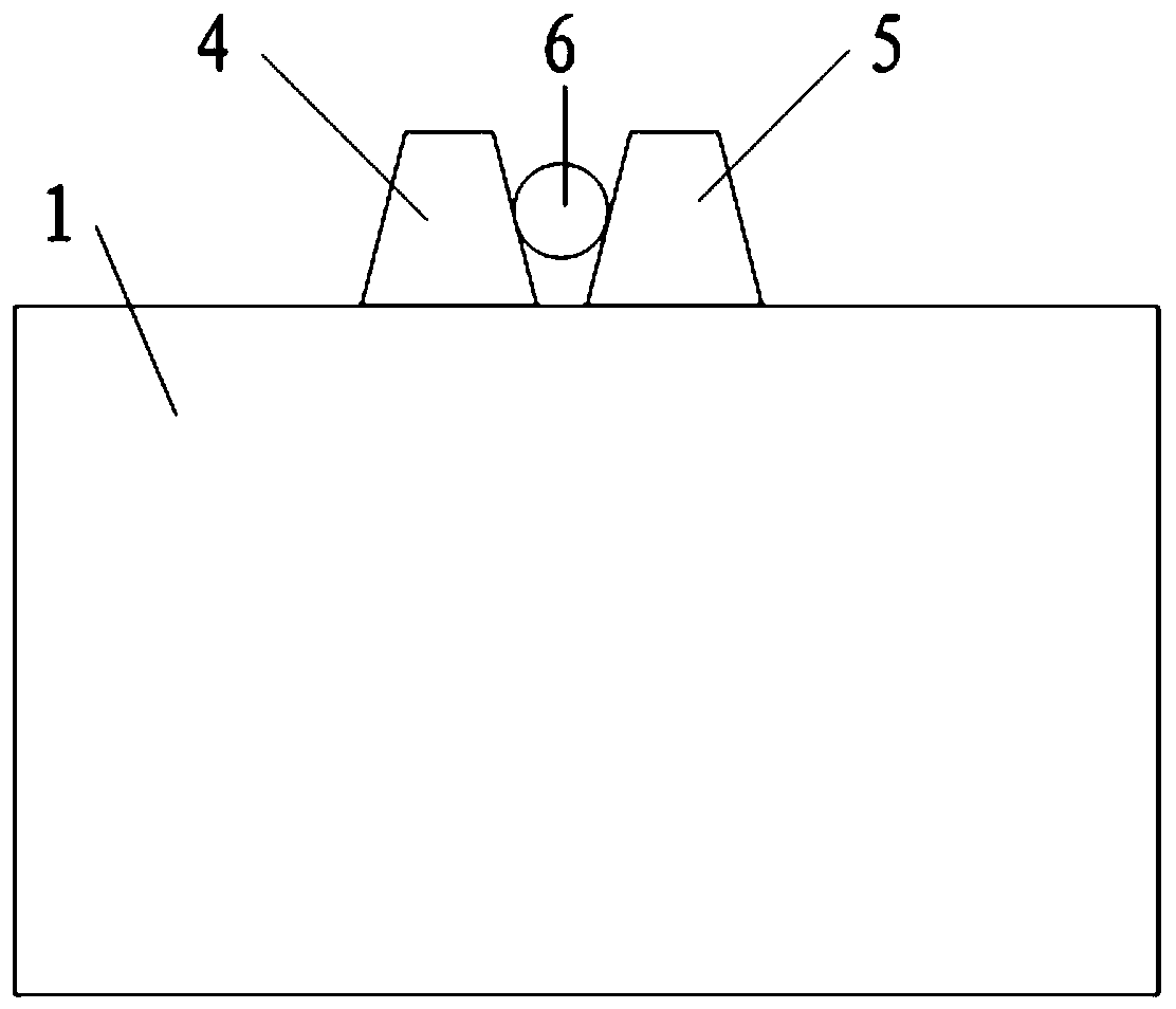
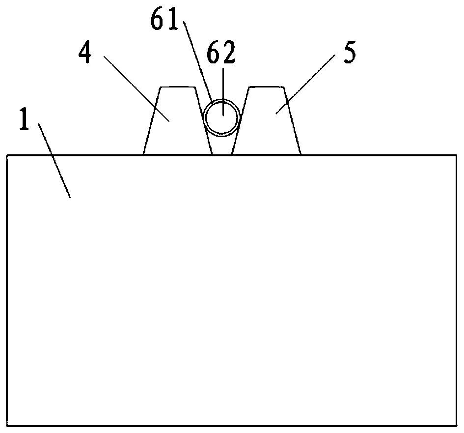
[0029] Embodiment 1: An electrically driven optical antenna light source integrated with a silicon-based optoelectronics circuit, specifically composed of figure 1 , figure 2 , image 3As shown, it includes a substrate 1, a first metal electrode 2, a second metal electrode 3, a first silicon waveguide 4, a second silicon waveguide 5 and an optical antenna 6, and the metal electrodes and the two silicon waveguides are all arranged on the surface of the substrate , the two silicon waveguides are respectively connected to two metal electrodes and a groove is formed between the two silicon waveguides; the optical antenna is located in the groove and is in contact with the two silicon waveguides, and the optical antenna includes metal nanoparticles 62 and is uniformly covered on A layer of insulating dielectric layer 61 on its outer surface. The entire optical antenna is composed of metal, and the entire optical antenna is composed of one or more nanoscale metal nanostructures. ...

Embodiment 2

[0031] The construction of the entire light source includes the following steps:

[0032] Firstly, a device model combining silicon waveguide and optical antenna is established for electromagnetic simulation experiments. Use numerical simulation software such as comsol or FDTD to construct the model structure of the entire device, use a dipole light source or a planar light source to excite the structure, confirm the optical response spectrum of the overall structure and the coupling efficiency of different wavelengths to the waveguide, and adjust the shape of the waveguide The appearance, size, material and structure of the optical antenna can be used to obtain the optimal situation.

[0033] In this embodiment, the entire device is constructed on an SOI substrate, and the substrate is, from top to bottom, a 220nm nano-device silicon layer, a 3-micron silicon oxide insulating layer, and a 500-micron silicon layer. The entire device is constructed from a 220nm device silicon ...


PUM

PropertyMeasurementUnit
thicknessaaaaaaaaaa

Abstract

The invention discloses an electrically-driven optical antenna light source and a manufacturing method thereof. The light source comprises an SOI substrate, metal electrodes, silicon waveguides and ananoscale optical antenna; the metal electrodes and the silicon waveguides are arranged on the surface of the SOI substrate; the metal electrodes are connected with the high-voltage end and the low-voltage end of an external connection circuit; the silicon waveguides are connected with the metal electrodes; a groove is formed between the silicon waveguides; and the optical antenna is located in the groove and is in contact with the two silicon waveguides; and the optical antenna comprises metal nanoparticles and an insulating dielectric layer uniformly covering the outer surface of the metal nanoparticles. The electrically-driven optical antenna light source of the invention has the advantages of high response speed, high coupling efficiency and high integration level.

Description

technical field [0001] The invention belongs to the technical field of silicon-based integrated light sources, and in particular relates to an electrically driven optical antenna light source and a manufacturing method thereof. Background technique [0002] Since silicon-based optoelectronic integrated circuits showed high-speed advantages in the 1990s, electrically excited on-chip light sources that can be directly integrated with silicon-based photonic circuits have become a development focus in this field. However, as silicon is an indirect bandgap semiconductor with a bandgap of 1.12eV, the excited electrons inside can only radiate photons when there is a direct interband transition or an intraband transition assisted by phonons or impurities. Most of these effects occur with extremely low probability, which directly hinders the development of silicon-based integrated light sources. At this stage, researchers have realized the integration of light sources by using silic...

Claims


Application Information

Patent Timeline
Patent Type & Authority Applications(China)
IPC IPC(8): H01L33/00
CPCH01L33/0037H01L33/0054
Inventor 张顺平唐继博胡华天何小波徐红星
Owner WUHAN UNIV
Why Eureka
Try Eureka