PCB, layout method and device thereof and storage medium

A PCB board, prohibiting wiring technology, applied in the field of PCB board design, can solve the problems of increasing PCB cost, unfavorable product miniaturization, etc., and achieve the effect of increasing current carrying capacity, reliable design principle, and saving wiring area

Active Publication Date: 2020-06-16
INSPUR SUZHOU INTELLIGENT TECH CO LTD
View PDF5 Cites 3 Cited by
  • Summary
  • Abstract
  • Description
  • Claims
  • Application Information

AI Technical Summary

Problems solved by technology

[0004] In the prior art, when a low-voltage and high-current circuit is encountered during PCB design, in order to meet the current-carrying capacity of the circuit, the PCB layer is usually increased or the PCB area is increased to widen the power plane of the power circuit, but this Both solutions will increase PCB cost and are not conducive to product miniaturization

Method used


Image

  • PCB, layout method and device thereof and storage medium
  • PCB, layout method and device thereof and storage medium

Examples


Embodiment 1

[0034] Such as figure 1 and 2 As shown, the present embodiment provides a PCB board, including:

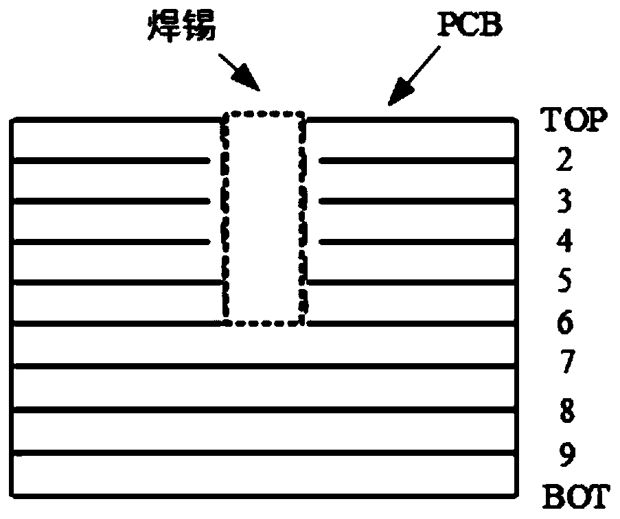
[0035] The PCB board body is provided with an inner layer power supply layer in the PCB board body, a top layer power supply layer is provided on the top layer of the PCB board body, and copper sheets are provided on both the inner layer power supply layer and the top layer power supply layer; There are milling slot holes, and a tin layer is plated in the milling slot holes. The bottom end of the tin layer is connected to the inner layer power layer, and the top end of the tin layer is connected to the top layer power layer. The signal layer is isolated from the tin layer.

Embodiment 2

[0037] Such as figure 1 and 2 As shown, a method for laying out a PCB board provided in this embodiment includes the following steps:
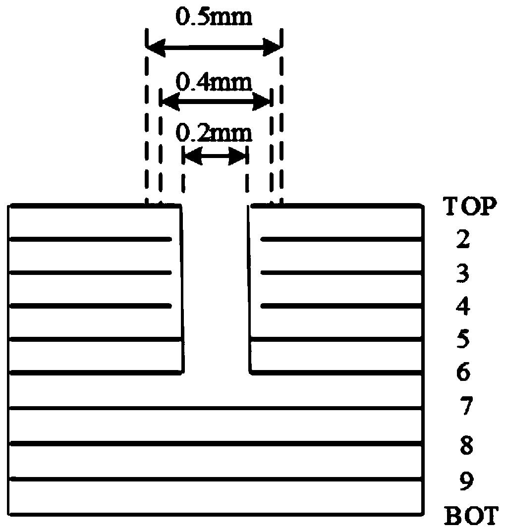
[0038] S1: In the bottleneck area of ​​the power transmission plane, along the current transmission direction, lay a copper sheet with a width of at least 0.5mm on the surface of the PCB; then lay a window area and a steel mesh area on the surface copper sheet; center on the surface copper sheet Set the silk screen label; lay a forbidden wiring area on the adjacent layer between the second outer layer and the power layer; the width of the window area is 0.4mm; the width of the steel mesh area is 0.5mm; the silk screen label width is 0.2mm; the wiring area is prohibited The width is 0.5mm.

[0039] S2: During PCB processing, use a milling cutter to mill grooves in the area marked by silk screen. The depth of the milling grooves only drills through the low-voltage and high-current power layer, and does not touch the next layer of the power pla...

Embodiment 3

[0043] Embodiment 3: This embodiment provides a layout device for PCB boards, including:

[0044] PCB surface layer laying module,

[0045] In the bottleneck area of ​​the power transmission plane, along the current transmission direction, lay a copper sheet with a width of at least 0.5mm on the surface of the PCB; then lay out the window area and the steel mesh area on the surface copper sheet; set the silk screen around the surface copper sheet Marking; Lay the forbidden wiring area on the adjacent layer between the second outer layer and the power layer;

[0046] slot milling module,

[0047] During PCB processing, use a milling cutter to mill the groove in the silk screen marked area. The depth of the milling groove only drills through the low-voltage and high-current power layer, and does not touch the next layer of the power plane;

[0048] tinned modules,

[0049] During PCB placement, the stencil area at the milling slot is partially thickened to increase the amount...


PUM


Abstract

The invention relates to a PCB and a layout method and device thereof, and a storage medium. The method comprises the steps of S1 laying a copper sheet on the surface layer of the PCB in a bottleneckregion of a power transmission plane in a current transmission direction; arranging a windowing area and a steel mesh area on the surface copper sheet; arranging a silk-screen label with the surface copper sheet as the center; laying a wiring forbidding area on an adjacent layer between the secondary outer layer and the power supply layer; S2 during PCB processing, carrying out silk-screen printing on a marking area , using a milling cutter for groove milling, wherein the groove milling depth only drills through the low-voltage large-current power supply layer, and the next layer of the powersupply plane is not contacted; and S3 finally, during PCB surface mounting, carrying out local thickening treatment on the steel mesh area at the milling groove, increasing the tinning amount in the milling groove, and finally, filling the groove hole with tin.

Description

technical field [0001] The invention belongs to the technical field of PCB board design, and in particular relates to a PCB board and its laying method, device and storage medium. Background technique [0002] With the development of electronic information, electronic products have more and more functions, and the power consumption of corresponding electronic components is gradually increasing, and it is also developing towards low voltage and high current. [0003] In the PCB design process, the power supply design is the focus and difficulty, especially for circuits with low voltage and high current. If the current carrying capacity of the circuit in the PCB design cannot meet the maximum current required by the system, it will inevitably lead to unstable operation of the entire circuit system. As electronic products tend to be more and more miniaturized, the PCB board area is gradually reduced. [0004] In the prior art, when a low-voltage and high-current circuit is en...

Claims


Application Information

Patent Timeline
Patent Type & Authority Applications(China)
IPC IPC(8): H05K1/02
CPCH05K1/0263H05K1/0265
Inventor 杨才坤
Owner INSPUR SUZHOU INTELLIGENT TECH CO LTD
Why Eureka
Try Eureka