Electron source substrate and display apparatus using it

a technology of display apparatus and substrate, which is applied in the direction of instruments, discharge tubes, tubes with screens, etc., can solve the problems of increasing the number of devices damaged by the discharge, affecting the quality of displayed images, and affecting the display apparatus using the conventional sce device described abov

Inactive Publication Date: 2006-08-29
CANON KK
View PDF20 Cites 11 Cited by
  • Summary
  • Abstract
  • Description
  • Claims
  • Application Information

AI Technical Summary

Benefits of technology

[0017]An object of the present invention is to solve the above problems, thereby providing an electron source substrate in which, even with occurrence of discharge between the anode and an electron-emitting device, the other electron-emitting devices are prevented from being negatively affected thereby, and display apparatus using it.

Problems solved by technology

The display apparatus using the conventional SCE devices described above had the problems as described below, however.
Conventionally, such phenomena posed the problem that nonuniformity of luminance or the like resulted in degradation of quality of displayed images.
The number of devices damaged by this discharge tends to increase with increase in the anode voltage.
For this reason, it was impossible to adequately increase the anode voltage heretofore, and this was a cause of decrease in the luminance of the display panel.

Method used


Image

  • Electron source substrate and display apparatus using it
  • Electron source substrate and display apparatus using it
  • Electron source substrate and display apparatus using it

Examples


example 1

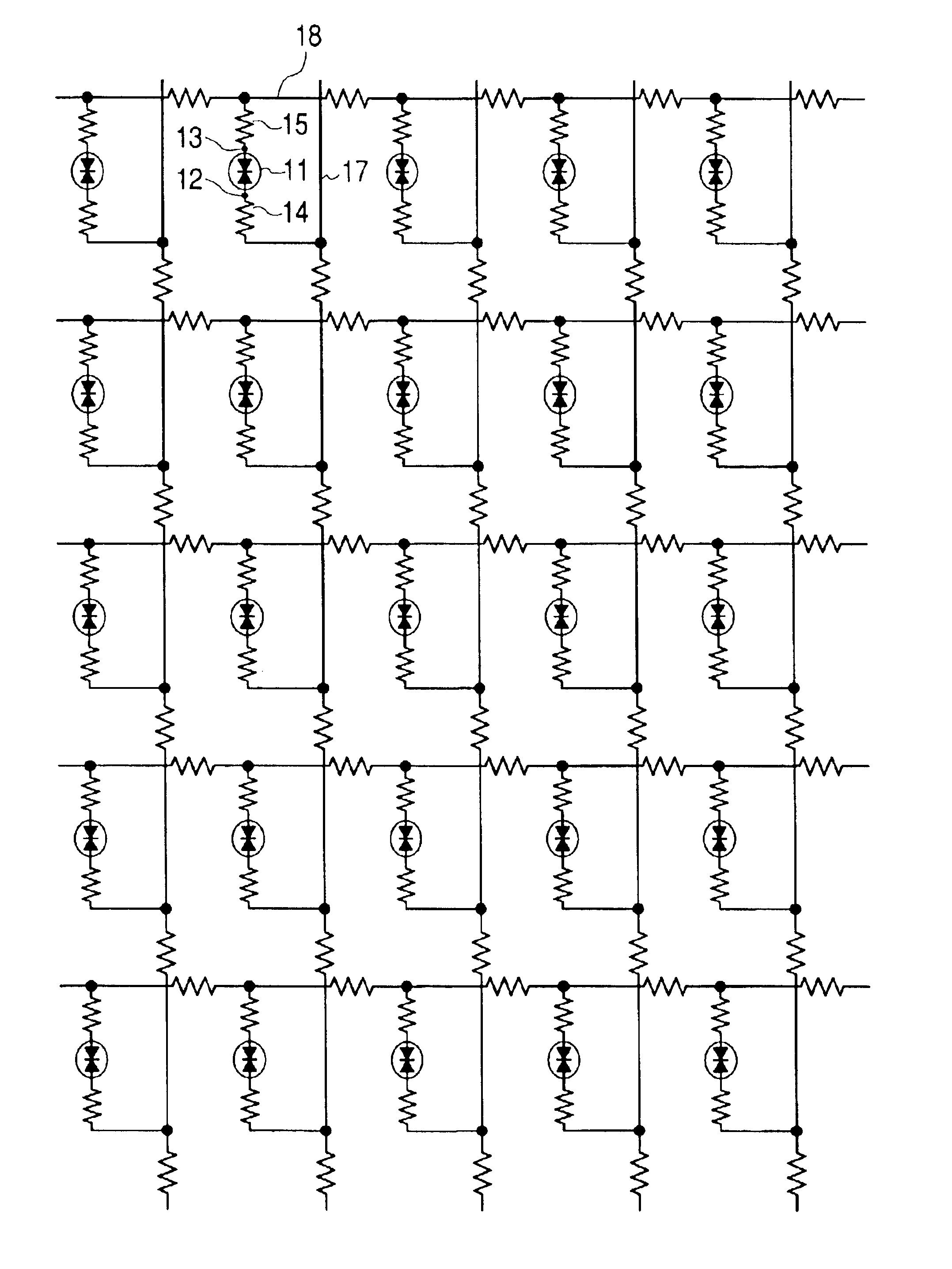
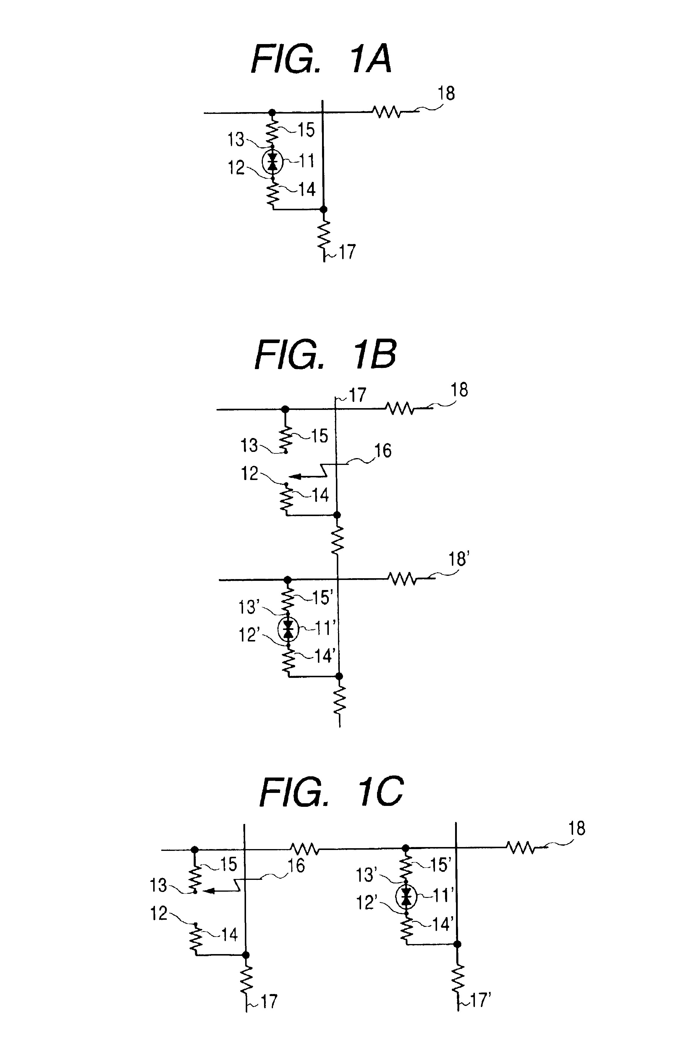
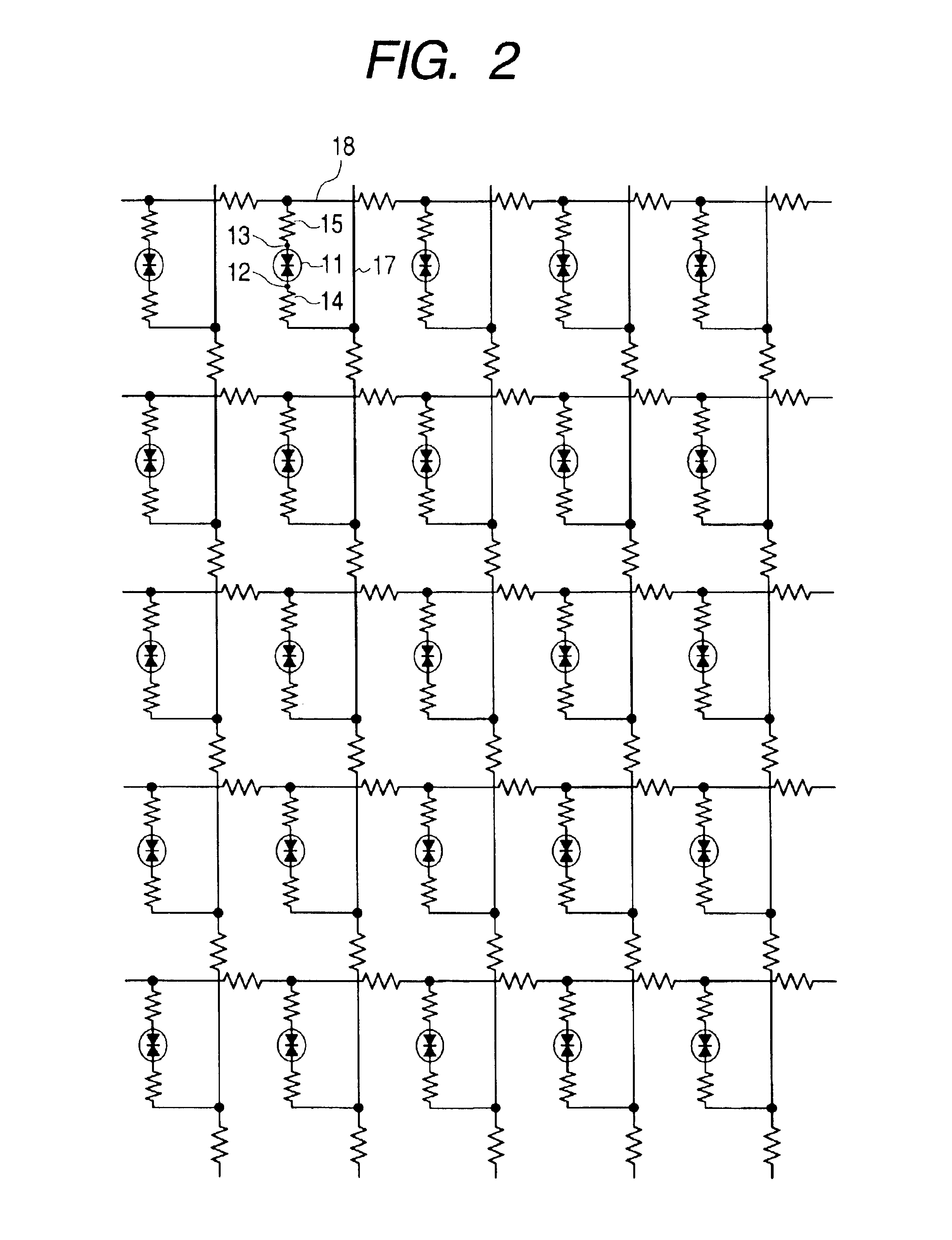
[0098]FIG. 3 is a schematic diagram showing a schematic configuration of the matrix wiring portion as an example of the electron source substrate according to the present invention. In FIG. 3, the electron-emitting devices 31, paired device electrodes 32, 33, first resistor elements 34, column-directional wiring lines 35, and row-directional wiring lines 36 are similar to those described with the aforementioned equivalent circuit diagram and are formed on the electron source substrate (rear plate) 30. Each electron-emitting device 31 has a pair of device electrodes 32, 33 and a device film is formed so as to connect these device electrodes. The device electrode 33 is coupled to the first resistor element 34, and the device electrode 32 to the second resistor element not shown. The second resistor element is located in a through hole formed in an insulating layer and is thus not shown in FIG. 3.

[0099]A method of producing this rear plate 30 will be described in order. FIGS. 4 to 9 ar...

example 2

[0147]In the present example, the resistor elements are formed only on the column-directional wiring side and the device electrodes also serve as the resistor elements. Specifically, the present example is different from aforementioned Example 1 in that the device electrodes are constructed of resistors, and the other structure is substantially the same as in Example 1. Therefore, only the part of the device electrodes will be described below in detail.

[0148]In the present example, in order to provide the device electrode coupled to the column-directional wiring with a desired resistance, the device electrode is made using a film of mixed materials of a metal and an insulator (which will be referred to hereinafter as a cermet film).

[0149]The metal used in the cermet film in the present example is platinum (Pt) and the insulator is silicon oxide (SiO2). The two materials are processed each into powder, they are mixed each in desired percent by weight, and a sputtering target is fabri...

example 3

[0153]In the present example, an additional resistor element and a specific break line are formed between the column-directional wiring and each device electrode in the configuration of Example 2 described above, and the electron source substrate is constructed in a configuration wherein, with occurrence of large-scale discharge, the specific break line is broken to shut off flow of the discharge current into the other devices more securely. The present example will be described below with FIG. 21.

[0154]FIG. 21 is a schematic configuration diagram (plan view) showing an example of the electron source substrate according to the present invention, which shows only part of the electron source substrate. In FIG. 21, numeral 1001 designates a substrate, 1002 and 1003 device electrodes, 1004 an electroconductive thin film in each device, 1005 an electron-emitting region in each device, 1006 and 1007 column-directional wiring and row-directional wiring coupled to the device electrodes 1002...


PUM


Abstract

There is provided an electron source substrate capable of, even with occurrence of discharge between an anode and an electron-emitting device, avoiding the negative effect on other electron-emitting devices. The electron source substrate has row-directional wiring laid in a row direction; column-directional wiring laid in a column direction so as to intersect with the row-directional wiring; and an electron-emitting device one end of which is coupled to the row-directional wiring, the other end of which is coupled through a resistor element to the column-directional wiring, and to which a predetermined drive voltage is supplied through the wiring, and is configured so that a wiring resistance of the column-directional wiring is higher than a wiring resistance of the row-directional wiring.

Description

BACKGROUND OF THE INVENTION[0001]1. Field of the Invention[0002]The present invention relates to an electron source substrate in which a plurality of electron-emitting devices are arranged in a matrix pattern, and display apparatus using it.[0003]2. Related Background Art[0004]As the electron-emitting devices used in the display apparatus of this type, there are two types of devices: thermal electron sources and cold cathode electron sources. The cold cathode electron sources include field emission devices, metal / insulator / metal devices, surface conduction electron-emitting devices (hereinafter referred to as SCE devices), and so on. The SCE devices will be described herein.[0005]The SCE devices are devices making use of the phenomenon in which electrons are emitted when an electric current is allowed to flow through a thin film of a small area formed on a substrate and in parallel to the film surface. FIGS. 19A and 19B show the configuration of the M. Hartwell's device as a typical...

Claims


Application Information

Patent Timeline
Patent Type & Authority Patents(United States)
IPC IPC(8): H01J9/04H01J1/30H01J29/04G09G3/22H01J1/316H01J29/96H01J31/12
CPCH01J29/96G09G3/22
Inventor KATAKURA, KAZUNORIHACHISU, TAKAHIRO
Owner CANON KK
Why Eureka
Try Eureka