Polishing thinning device and polishing thinning method

A technology of polishing liquid and photoresist, which is applied in grinding devices, grinding/polishing equipment, grinding machine tools, etc., can solve problems such as wafer fragmentation, poor physical properties of InP materials, and fragility, and reduce extrusion stress , Reduce the effect of machining damage

Inactive Publication Date: 2020-06-19
INST OF MICROELECTRONICS CHINESE ACAD OF SCI
View PDF9 Cites 0 Cited by
  • Summary
  • Abstract
  • Description
  • Claims
  • Application Information

AI Technical Summary

Problems solved by technology

[0004] However, the physical properties of InP materials are very poor, and they are very fragile. A small impact or vibration will cause the wafer to break and all previous efforts will be wasted. Therefore, the manufacturing and processing of InP materials is facing many technological difficulties.

Method used


Image

  • Polishing thinning device and polishing thinning method
  • Polishing thinning device and polishing thinning method
  • Polishing thinning device and polishing thinning method

Examples


Embodiment Construction

[0037] The above is the core idea of ​​the present invention. In order to make the above-mentioned purposes, features and advantages of the present invention more obvious and easy to understand, the technical solutions in the embodiments of the present invention will be clearly and completely described below in conjunction with the accompanying drawings in the embodiments of the present invention Description, obviously, the described embodiments are only a part of the embodiments of the present invention, rather than all the embodiments. Based on the embodiments of the present invention, all other embodiments obtained by persons of ordinary skill in the art without making creative efforts belong to the protection scope of the present invention.

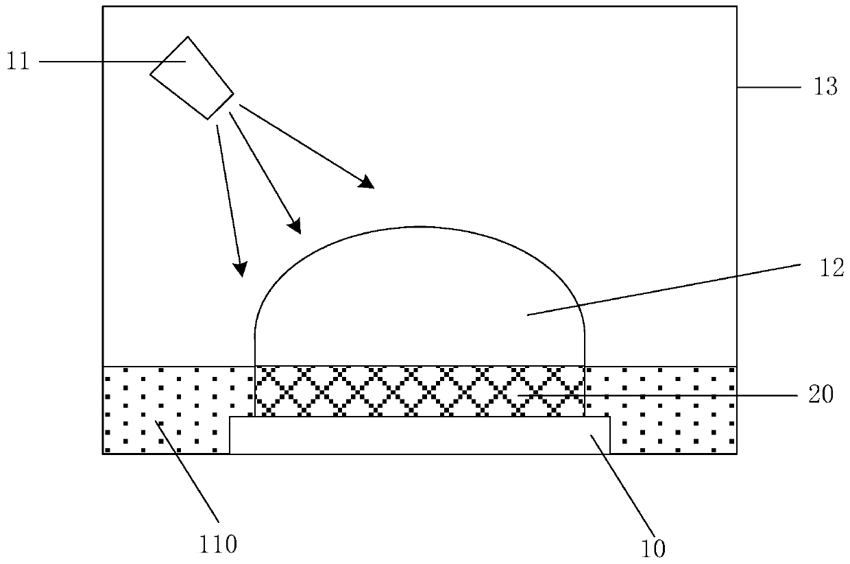
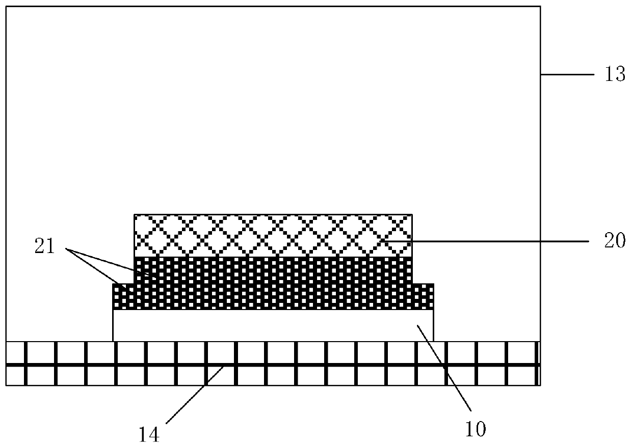
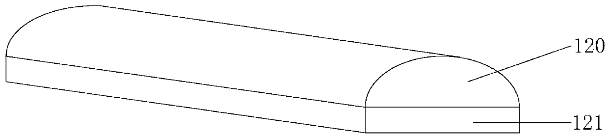
[0038] An embodiment of the present invention provides a polishing and thinning device for polishing and thinning components such as InP-based wafers, such as figure 1 As shown, it includes a tray 10, a shower head 11 and a magnetic r...


PUM

PropertyMeasurementUnit
diameteraaaaaaaaaa

Abstract

The invention provides a polishing thinning device and a polishing thinning method. The device comprises a tray, a spray head and a magnetic rotor. The tray is used for fixing a part to be machined, and the part to be machined comprises an InP-based wafer; the spray head is used for spraying polishing liquid to the surface to be machined of the part to be machined so as to polish the surface to bemachined; and the magnetic rotor is arranged on the surface to be machined of the part to be machined and used for mechanically grinding the surface to be machined through rotation and thinning the surface to be machined. Since the part to be processed such as the InP-based wafer does not rotate in the thinning process, the extrusion stress on the part to be machined such as the InP-based wafer in the polishing thinning process can be greatly reduced, and the machining damage to the part to be machined such as the InP-based wafer can be greatly reduced.

Description

technical field [0001] The invention relates to the technical field of semiconductor manufacturing, and more specifically, to a polishing and thinning device and a polishing and thinning method. Background technique [0002] Semiconductor devices and ultra-high-speed digital / digital-analog hybrid circuits made of III-V compounds have become modern defense equipment such as military communications, radar, guidance, space defense, high-speed intelligent weapons, and electronic countermeasures due to their excellent frequency characteristics. One of the core components. [0003] Among the numerous III-V compounds, InP (indium phosphide) compounds have unique advantages, mainly due to their excellent material properties, for example, the lattice mismatch between InP and InGaAs (indium gallium arsenide) It is very small, and the electron saturation rate is very high, so whether it is a HEMT (High Electron Mobility Transistor, high electron mobility transistor) structure or a HBT...

Claims


Application Information

Patent Timeline
Patent Type & Authority Applications(China)
IPC IPC(8): B24B37/10B24B37/30B24B37/34B24B57/02H01L21/304
CPCB24B37/042B24B37/107B24B37/30B24B37/34B24B57/02H01L21/304
Inventor 汪宁
Owner INST OF MICROELECTRONICS CHINESE ACAD OF SCI
Why Eureka
Try Eureka