
Backlight module and preparation method thereof and display device

A technology for backlight modules and light-emitting devices, which is used in identification devices, semiconductor/solid-state device manufacturing, instruments, etc., can solve the problems of poor electrical conductivity, long time, and the loss of the lap function of vias, so as to solve the problems of poor electrical conductivity, Increases adhesion, reduces the effect of process steps

Active Publication Date: 2020-06-19
SHENZHEN CHINA STAR OPTOELECTRONICS SEMICON DISPLAY TECH CO LTD
View PDF7 Cites 9 Cited by
  • Summary
  • Abstract
  • Description
  • Claims
  • Application Information

AI Technical Summary

Problems solved by technology

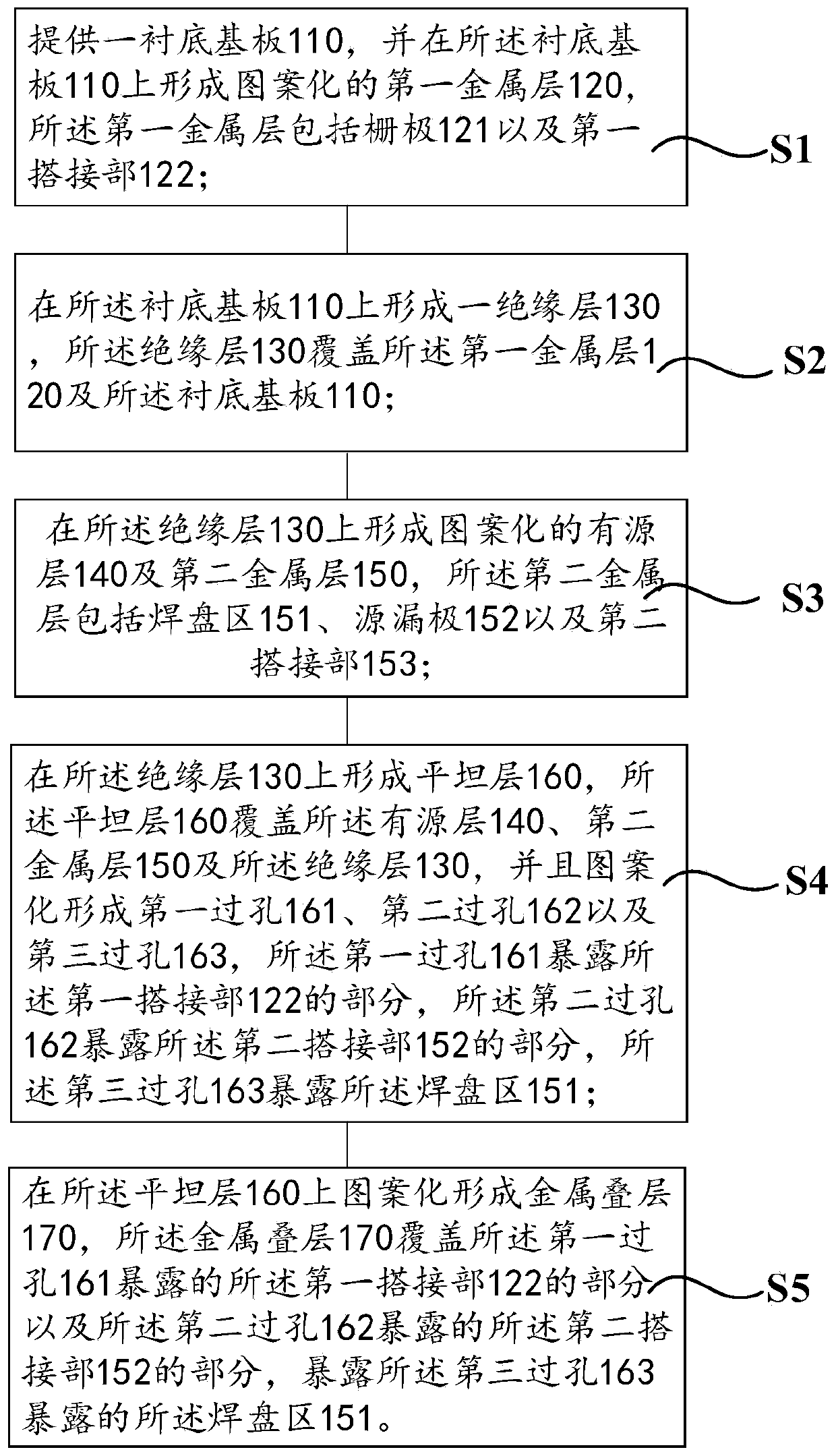
[0005] The purpose of the present invention is to provide a backlight module, its preparation method, and a display device, so as to solve the technical problems in the prior art that ITO has poor electrical conductivity and the via holes lose their overlapping function due to aging after a long time or high temperature. , while effectively reducing light loss and energy consumption

Method used


Image

  • Backlight module and preparation method thereof and display device
  • Backlight module and preparation method thereof and display device
  • Backlight module and preparation method thereof and display device

Examples


Embodiment Construction

[0035] The technical solutions in the embodiments of the present application will be clearly and completely described below in conjunction with the drawings in the embodiments of the present application. Apparently, the described embodiments are only some of the embodiments of this application, not all of them. Based on the embodiments in this application, all other embodiments obtained by those skilled in the art without making creative efforts belong to the scope of protection of this application.

[0036] In the description of the present application, it should be understood that the terms "center", "longitudinal", "transverse", "length", "width", "thickness", "upper", "lower", "front", " Orientation indicated by rear, left, right, vertical, horizontal, top, bottom, inside, outside, clockwise, counterclockwise, etc. The positional relationship is based on the orientation or positional relationship shown in the drawings, which is only for the convenience of describing the a...


PUM

PropertyMeasurementUnit
thicknessaaaaaaaaaa
reflectanceaaaaaaaaaa

Abstract

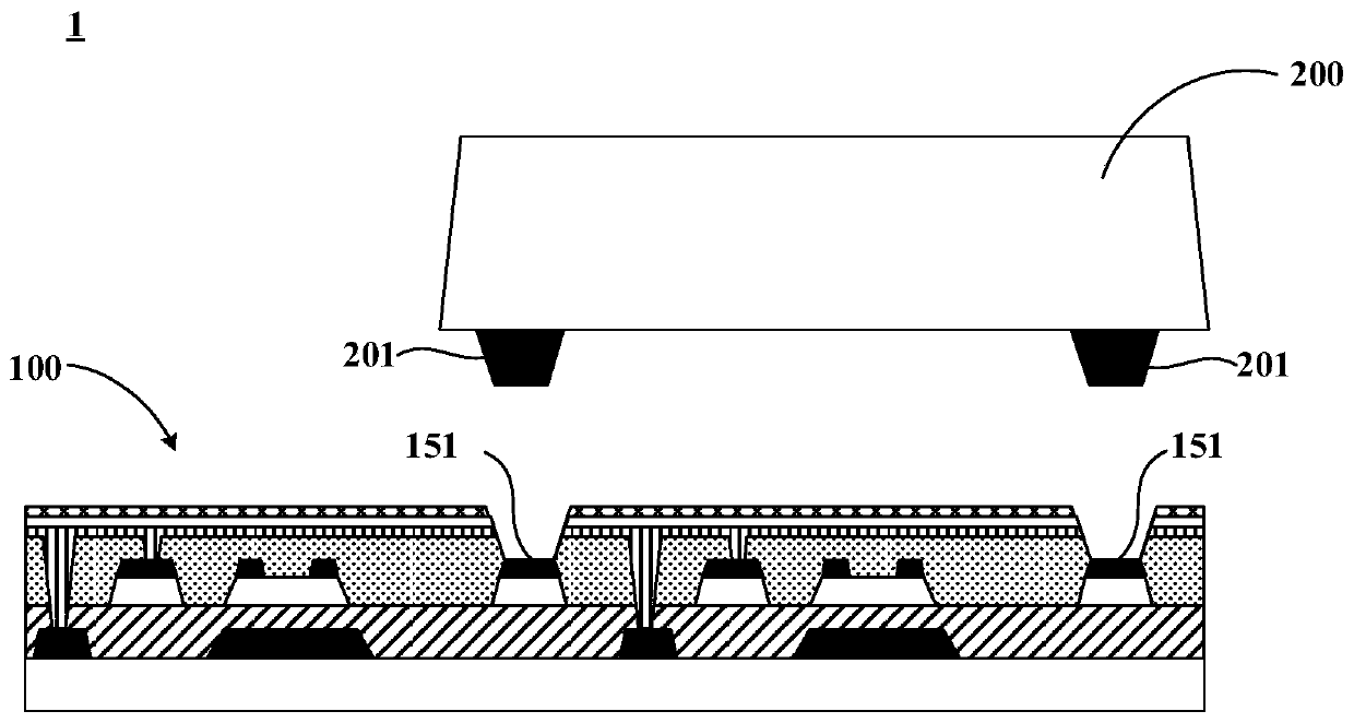
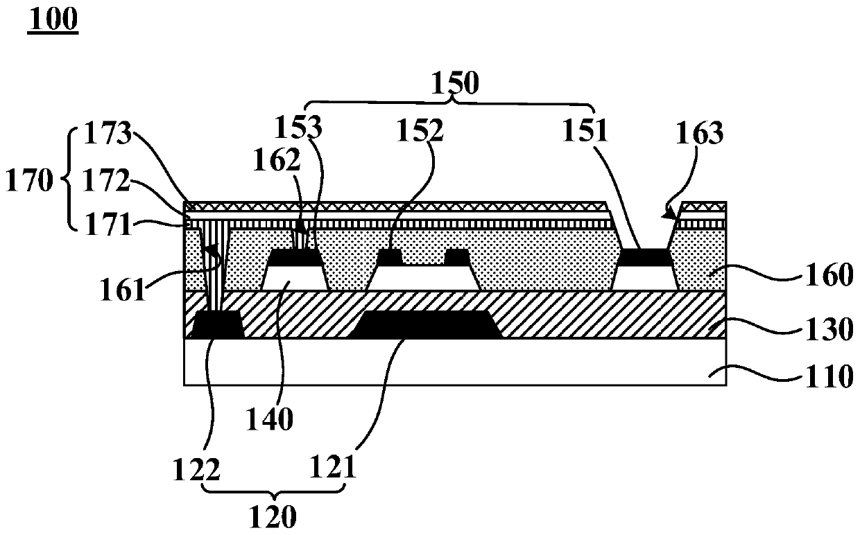
The invention discloses a backlight module and a preparation method thereof and a display device. The backlight module comprises an array substrate and a plurality of light-emitting devices arranged on the array substrate, and the array substrate comprises an underlying substrate and a first metal layer and a second metal layer which are arranged on the underlying substrate; a flat layer which covers the first metal layer and the second metal layer and exposes a part of the first metal layer and a part of the second metal layer; and a metal lamination layer which is arranged on the flat layerand is in contact with the part, exposed out of the flat layer, of the first metal layer and the part, exposed out of the flat layer, of the second metal layer, wherein the metal lamination layer comprises at least one layer of first metal, at least one layer of second metal and at least one layer of metal oxide, and the first metal is molybdenum. The second metal has high-strength reflectivity, and the conductivity of the second metal is superior to that of the metal oxide so that the optical loss can be effectively reduced and better conductivity is achieved.

Description

technical field [0001] The present application relates to the field of display technology, in particular to a backlight module, a manufacturing method thereof, and a display device. Background technique [0002] With the development of display technology, Micro-LED (Micro-Light Emitting Diode, miniature light-emitting diode) has developed into one of the hot spots of future display technology, and the current LCD (Liquid Crystal Display, liquid crystal display), OLED (Organic Light Emitting Diode, organic Compared with light-emitting diode) display devices, it has the advantages of fast response, high color gamut, high PPI (Pixels Per Inch, pixel density), low energy consumption, etc.; but its technical difficulties are many and complex, especially its key technology mass transfer technology , LED (Light Emitting Diode, light-emitting diode) particle miniaturization has become a technical bottleneck, and Mini-LED (Mini-Light Emitting Diode, mini light-emitting diode), as the...

Claims


Application Information

Patent Timeline
Patent Type & Authority Applications(China)
IPC IPC(8): H01L27/15H01L27/12H01L21/768G09F9/33
CPCH01L27/156H01L27/1244H01L27/124H01L27/1259H01L21/76838G09F9/33
Inventor 王明耀刘俊领
Owner SHENZHEN CHINA STAR OPTOELECTRONICS SEMICON DISPLAY TECH CO LTD
Learn More