Meter-level large-aperture optical components co 2 Laser polishing device and polishing method

A technology for optical components and laser polishing, which is applied in laser welding equipment, metal processing equipment, welding equipment, etc., can solve problems that affect the service life of optical components, easily induce defects, and pollute the environment, so as to improve the repair effect and improve polishing The effect of precision and easy operation

Active Publication Date: 2022-05-20
NANJING UNIV OF SCI & TECH
View PDF8 Cites 0 Cited by
  • Summary
  • Abstract
  • Description
  • Claims
  • Application Information

AI Technical Summary

Problems solved by technology

Traditional optical components generally need to go through blanking, grinding, rough polishing, semi-finish polishing, fine polishing and other processes, especially the grinding and polishing process, which not only takes a long time, pollutes the environment, but also causes impurities to penetrate into the processed components. , affecting the service life of optical components, especially under the action of strong laser light, trace impurities can easily induce defects after repeated actions, resulting in component damage or even scrapping

Method used


Image

  • Meter-level large-aperture optical components co  <sub>2</sub> Laser polishing device and polishing method
  • Meter-level large-aperture optical components co  <sub>2</sub> Laser polishing device and polishing method
  • Meter-level large-aperture optical components co  <sub>2</sub> Laser polishing device and polishing method

Examples


Embodiment

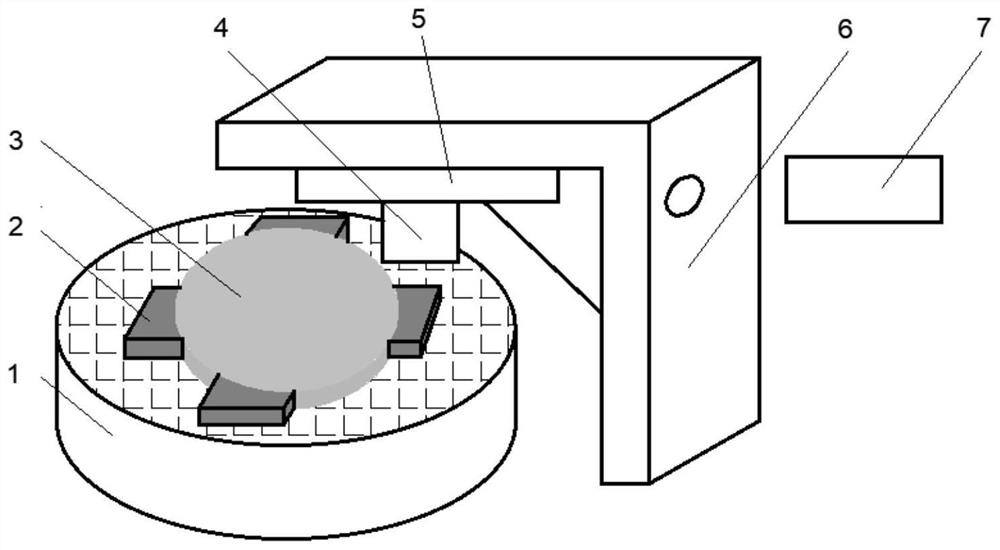
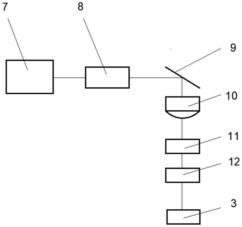
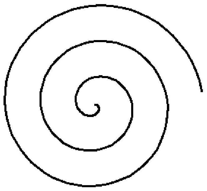
[0032] CO for meter-scale large-aperture optical components 2 Laser polished, the base material is round fused silica glass. The experiment was carried out in a class 10,000 clean room. First, the optical components are cleaned and dried for pretreatment. Then the optical element 3 is fixed on the workbench 1 through the electromagnetic clamp 2, and the optical element 3 faces the laser beam. Adjust laser parameters: laser power 60W, repetition frequency 1kHz, pulse width 10μs, focal length 20mm, spot diameter 2mm, galvanometer scanning speed 100mm / s, track interval 1mm, track exceeding fused silica size by 1%. The speed of workbench 1 is 1rad / s, the speed of the feed mechanism is 5mm / s, and the attachment image 3 Scanning in a spiral trajectory. After scanning the entire surface of the optical element, reduce the laser power by 5-10W each time, reduce the speed of the feed mechanism by 5-10mm / s, and keep the other parameters unchanged. Repeat multiple scans until the sur...


PUM


Abstract

The invention relates to a meter-level large-aperture optical element CO 2 Laser polishing device. On the basis of moving the optical components at a uniform speed on the workbench, the laser beam passes through the hole on the bracket, and the beam is transmitted to the vibrating mirror system composed of the vibrating mirror and the focusing mirror through the reflector to realize the processing of the optical components. There is an integrated reflector, galvanometer, and focusing mirror to move linearly in the direction of laser incident from the hole, and the optical transmission will not be affected by the movement of the galvanometer system, so that the combination of worktable movement and galvanometer system movement is well realized. Coarse positioning of the motion track, the movement of the galvanometer system itself realizes the fine positioning of the motion track. The device of the invention scans the optical element by means of a spiral processing track and changes parameters, and realizes the polishing of the surface of the optical element by means of a combination of melting and gasification. The device of the invention can realize linear or circular motion above the meter level.

Description

technical field [0001] The invention relates to the technical field of surface precision and ultra-precision processing of optical elements, in particular to meter-level large-diameter optical elements CO 2 Laser polishing device and polishing method. Background technique [0002] With the development of space optics, aerospace and other science and technology, higher and higher requirements are put forward for precision optical planar components. Not only the precision requirements are getting higher and higher, but also the size is getting larger and larger, which poses new challenges to the manufacture of optical components. . Traditional optical components generally need to go through blanking, grinding, rough polishing, semi-finish polishing, fine polishing and other processes, especially the grinding and polishing process, which not only takes a long time, pollutes the environment, but also causes impurities to penetrate into the processed components. , affects the s...

Claims


Application Information

Patent Timeline
Patent Type & Authority Patents(China)
IPC IPC(8): B23K26/352B23K26/70B23K26/00
CPCB23K26/352B23K26/70B23K26/00B23K26/702
Inventor 李晓鹏陆广华支新涛王大森王克鸿袁松梅周琦彭勇
Owner NANJING UNIV OF SCI & TECH
Why Eureka
Try Eureka