Light-emitting diode based on hole adjustment layer

A light-emitting diode and hole adjustment technology, which is applied to electrical components, circuits, semiconductor devices, etc., can solve problems such as affecting the luminous efficiency of light-emitting diodes, and achieve the effects of improving luminous efficiency, improving hole concentration, and improving luminous quality.

Inactive Publication Date: 2020-06-23
XIAN ZHISHENG RUIXIN SEMICON TECH CO LTD
View PDF0 Cites 3 Cited by
  • Summary
  • Abstract
  • Description
  • Claims
  • Application Information

AI Technical Summary

Problems solved by technology

[0004] However, the current light-emitting diodes still have problems such as many defects, and the quality of light emission needs to be further improved, so as not to affect the entry into the high-end application market; because the mobility of electrons is much higher than that of holes, the electron concentration in the multi-quantum well light-emitting layer Much higher than the concentration of holes, thus affecting the luminous efficiency of light-emitting diodes

Method used


Image

  • Light-emitting diode based on hole adjustment layer

Examples


Embodiment Construction

[0032] In order to make the above objects, features and advantages of the present invention more comprehensible, specific implementations of the present invention will be described in detail below in conjunction with the accompanying drawings.

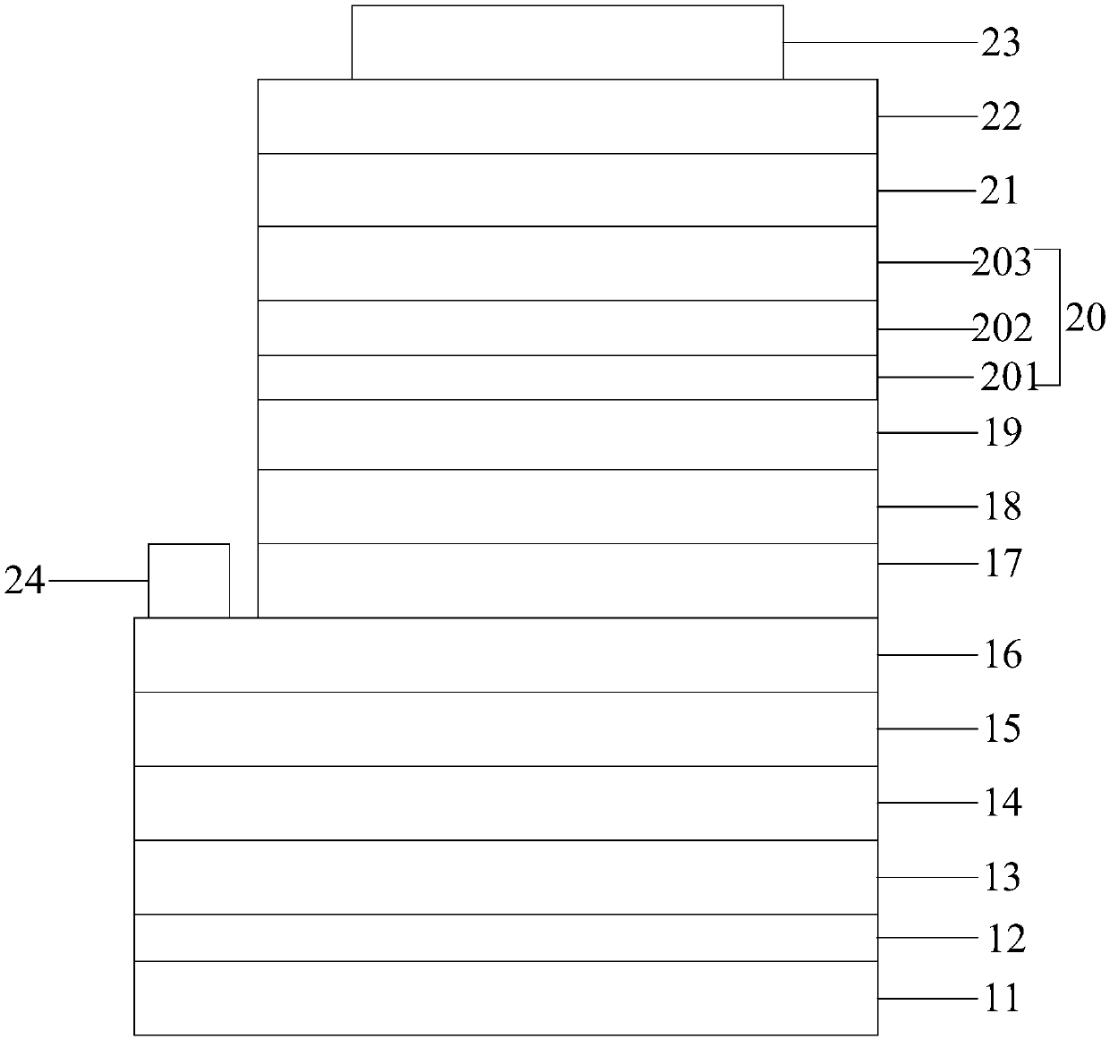
[0033] See figure 1 , figure 1 A schematic structural diagram of a light-emitting diode based on a hole adjustment layer provided by an embodiment of the present invention. An embodiment of the present invention provides a light-emitting diode based on a hole adjustment layer, the light-emitting diode comprising:

[0034] substrate layer 11;

[0035] Specifically, the material of the substrate layer 11 may be sapphire, silicon, silicon carbide, zinc oxide, gallium nitride, aluminum nitride or other materials suitable for crystal epitaxial growth.

[0036] The buffer layer 12 is located on the substrate layer 11;

[0037] Further, the material of the buffer layer 12 is GaN.

[0038] In the embodiment of the present invention, by gr...


PUM

PropertyMeasurementUnit
thicknessaaaaaaaaaa
thicknessaaaaaaaaaa
thicknessaaaaaaaaaa

Abstract

The invention relates to a light-emitting diode based on a hole adjustment layer. The light-emitting diode comprises a substrate layer, a buffer layer located on the substrate layer, a low-temperaturegallium nitride layer located on the buffer layer, an unintentionally doped gallium nitride layer located on the low-temperature gallium nitride layer, a superlattice layer located on the unintentionally doped gallium nitride layer, an N-type semiconductor layer located on the superlattice layer, an N-type doped layer located on the N-type semiconductor layer, a quantum well light-emitting layerlocated on the N-type doped layer, an electron blocking layer located on the quantum well light-emitting layer, a hole adjusting layer comprising a first non-doped layer, a second non-doped layer anda P-type doped layer which are sequentially laminated on the electron blocking layer, and a P-type semiconductor layer located on the hole adjusting layer. According to the light-emitting diode, the light emitting quality of the light-emitting diode can be improved. The hole concentration of holes migrated to the quantum well light-emitting layer can be improved, so that the light-emitting efficiency of the light-emitting diode is improved.

Description

technical field [0001] The invention relates to the technical field of light-emitting elements, in particular to a light-emitting diode based on a hole adjustment layer. Background technique [0002] LED (Light Emitting Diode, Light Emitting Diode) is a very influential new product in the emerging industry of information optoelectronics. It has the characteristics of small size, long service life, colorful colors, and low energy consumption. It is widely used in lighting, display screens, and signal lights. , backlight, toys and other fields. [0003] At present, a light-emitting diode generally includes a substrate layer, a buffer layer, an N-type semiconductor layer, a multi-quantum well light-emitting layer, and a P-type semiconductor layer. Among them, the N-type semiconductor layer is used to provide electrons; the P-type semiconductor layer is used to provide holes. When a current passes through, the electrons provided by the N-type semiconductor layer and the holes p...

Claims


Application Information

Patent Timeline
Patent Type & Authority Applications(China)
IPC IPC(8): H01L33/12H01L33/04H01L33/06H01L33/14
CPCH01L33/04H01L33/06H01L33/12H01L33/14H01L33/145
Inventor 李建华李全杰刘向英
Owner XIAN ZHISHENG RUIXIN SEMICON TECH CO LTD
Why Eureka
Try Eureka