Method for reducing coupling interference of electrostatic micro-mirror angle detection sensor

An angle detection and coupling interference technology, applied in the field of micro-nano optical devices, can solve the problems of high requirements for detection signal processing circuits, detection signal coupling interference, and reduction of detection accuracy, so as to improve the control accuracy of micromirrors, reduce the complexity, The effect of improving the signal-to-noise ratio

Active Publication Date: 2020-06-30
XIAN CHISHINE OPTOELECTRONICS TECH CO LTD
View PDF11 Cites 7 Cited by
  • Summary
  • Abstract
  • Description
  • Claims
  • Application Information

AI Technical Summary

Problems solved by technology

However, there is a serious problem in the current micromirror that is electrostatically driven and uses a capacitive sensor for angle detection. The driving capacitor and the detecting capacitor form a series capacitor circuit, and the driving signal generates a large coupling interference to the detection signal, and the signal-to-noise ratio is very low. The detection accuracy is reduced, and the requirements for the processing circuit of the detection signal are very high

Method used


Image

  • Method for reducing coupling interference of electrostatic micro-mirror angle detection sensor
  • Method for reducing coupling interference of electrostatic micro-mirror angle detection sensor
  • Method for reducing coupling interference of electrostatic micro-mirror angle detection sensor

Examples


Embodiment 1

[0039] Embodiment 1 micromirror design

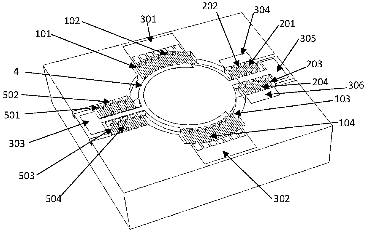
[0040] Such as Figure 4 Shown is a micromirror design, the mirror surface is circular, and the side of the mirror surface is provided with a first rotating comb 102 and a second rotating comb 104, which are respectively connected with the first fixed comb 101 and the third fixed comb fixed on the outer frame. The comb teeth 103 are staggered to form two groups of driving comb teeth. A rotating shaft is arranged in a direction perpendicular to the line connecting the rotating comb teeth, one end of the rotating shaft is connected to the circular mirror, and the other end is connected to the peripheral frame. A first movable detection comb 202 and a second movable detection comb 204 , a first movable balance comb 501 and a second movable balance comb 503 are arranged on the side of the rotating shaft. The first movable detection comb 202 and the second movable detection comb 204 respectively interleave with the first fixed detection co...

Embodiment 2

[0041] Embodiment 2 micromirror design

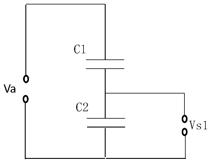
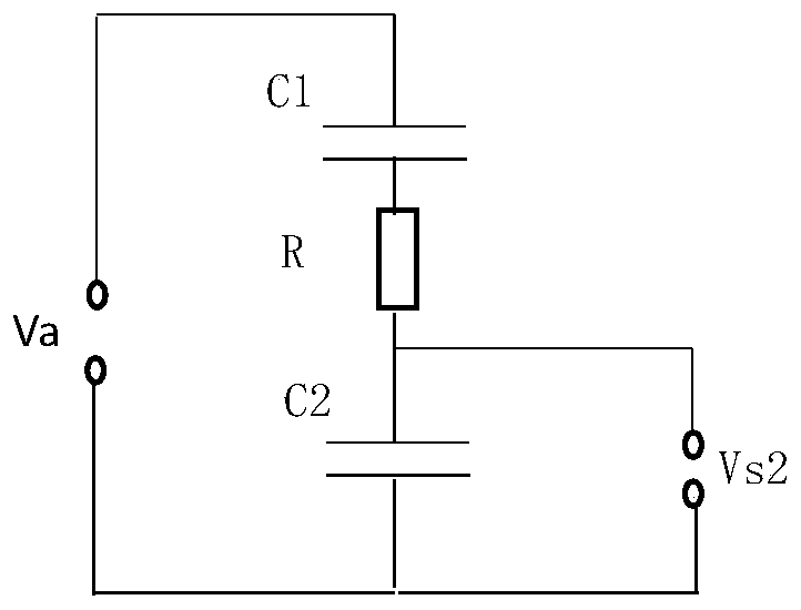
[0042] Such as Figure 5 Shown is a micromirror design, the difference from Example 1 is that the mirror surface is rectangular, all driving combs, detection combs and corresponding lead areas are doped, and then all driving combs, detection combs The teeth, pad areas and corresponding lead areas are deposited with an aluminum metal layer with a thickness of 500nm. According to the principle of resistance-capacitance voltage division, the coupling interference caused by the driving signal to the detection signal is Vs2=Va XC2 / (XC1+XC2+R), where XC1 and XC2 are the capacitive reactances of C1 and C2 respectively, and C1=C2=C, then XC1=XC2=1 / 2πfC, where f is the drive signal frequency, which is 2kHz in the present embodiment; C=NεS / d, where N is the logarithm of the comb teeth, which is 100 in the present embodiment; ε is the air permittivity, The value is 8.85×10 -12 F / m; S is comb tooth side area, is 2 * 10 in the present embodiment ...

Embodiment 3

[0043] Embodiment 3 Micromirror manufacturing method

[0044] In order to better illustrate the manufacturing method of the micromirror of the present invention, a specific operation process after the existing manufacturing method is added to the method of the present invention is listed. Such as Image 6

[0045] A method for making a micromirror that reduces the coupling interference of an electrostatic micromirror angle detection sensor:

[0046] (1) Prepare SOI (Silicon On Insulator) silicon wafer. The SOI silicon wafer includes a three-layer structure of base silicon 701 , buried oxide layer 702 and top layer silicon 703 from bottom to top. The base silicon 701 and the top layer silicon 703 are high-resistance silicon, and the resistivity range is 1-10 8 Ω·cm. The thickness of the base silicon 701 is 100-800 μm, the thickness of the buried oxide layer is 0.5-10 μm, and the thickness of the top layer is 5 μm-100 μm. Preferably, the base silicon 701 has a thickness of...


PUM

PropertyMeasurementUnit
electrical resistivityaaaaaaaaaa
thicknessaaaaaaaaaa
thicknessaaaaaaaaaa

Abstract

For improving the impedance of an equivalent coupling circuit and obviously reducing coupling interference of the driving signal on the detection signal, the invention provides a method for reducing coupling interference of an electrostatic micro-mirror angle detection sensor. Specifically, in the process of manufacturing the micro-mirror by adopting a high-resistivity semiconductor material, element doping is carried out on driving comb teeth and detection comb teeth of the micro-mirror and a lead area between the comb teeth and a bonding pad, then a micro-mirror structure is etched, and finally the micro-mirror capable of reducing the coupling interference of the angle detection sensor is obtained. According to the method, the coupling interference of the driving signal in the electrostatic micromirror on the angle detection signal can be remarkably reduced, the signal-to-noise ratio of the detection signal is improved, and the complexity of a processing circuit is reduced. Meanwhile, the method does not need to change the structure of the micro-mirror, and greatly improves the control precision of the micro-mirror on the basis of the same structure and similar process difficulty.

Description

technical field [0001] The invention relates to the field of micro-nano optical devices, in particular to a method for reducing the coupling interference of an electrostatic micro-mirror angle detection sensor. Background technique [0002] Micromirror is a kind of micro-nano chip that can effectively control the optical path, and is widely used in projection, imaging, laser navigation and other fields. At present, the most widely used micromirrors include electrostatic, electromagnetic, piezoelectric and electrothermal. Most of the currently used micromirrors adopt the open-loop control method without angle feedback. A serious shortcoming of this kind of micromirror is the lack of effective angle feedback, which causes the problem of inaccurate control of the micromirror, which leads to projection and imaging drift. , Navigation deviation and other issues. Some existing micromirrors use a certain angle feedback, but there are still many problems. [0003] For the current...

Claims


Application Information

Patent Timeline
Patent Type & Authority Applications(China)
IPC IPC(8): B81C1/00B81B7/00
CPCB81C1/00023B81C1/005B81C1/00642B81B7/00B81B2201/02B81C2201/0111Y02P70/50
Inventor 李欢欢白民宇马力彭磊郭迪王丛华
Owner XIAN CHISHINE OPTOELECTRONICS TECH CO LTD
Why Eureka
Try Eureka