Si-based modified Ge monolithic same-layer photoelectric device

An optoelectronic device and modification technology, applied in the field of microelectronics, can solve the problems of long process cycle, process incompatibility, and high production cost, and achieve the effects of high electron mobility, improved luminous efficiency, and reduced production cost.

Inactive Publication Date: 2020-06-30
XIAN CREATION KEJI CO LTD
View PDF0 Cites 0 Cited by
  • Summary
  • Abstract
  • Description
  • Claims
  • Application Information

AI Technical Summary

Problems solved by technology

[0004] In the field of optoelectronic devices, III-V semiconductor materials have been widely used, but they are not compatible with the existing Si process, and their high production cost and long process cycle restrict their further development.

Method used


Image

  • Si-based modified Ge monolithic same-layer photoelectric device
  • Si-based modified Ge monolithic same-layer photoelectric device
  • Si-based modified Ge monolithic same-layer photoelectric device

Examples


Embodiment 1

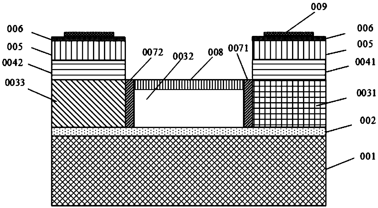
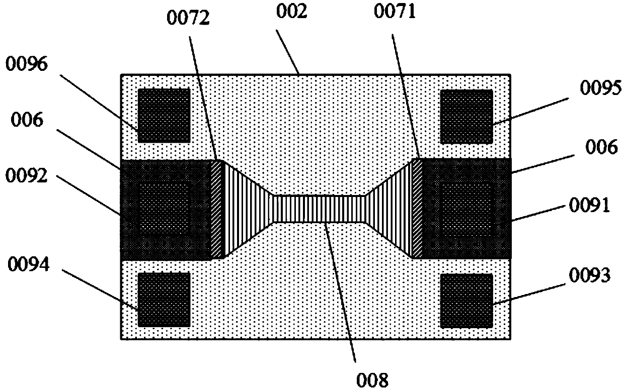
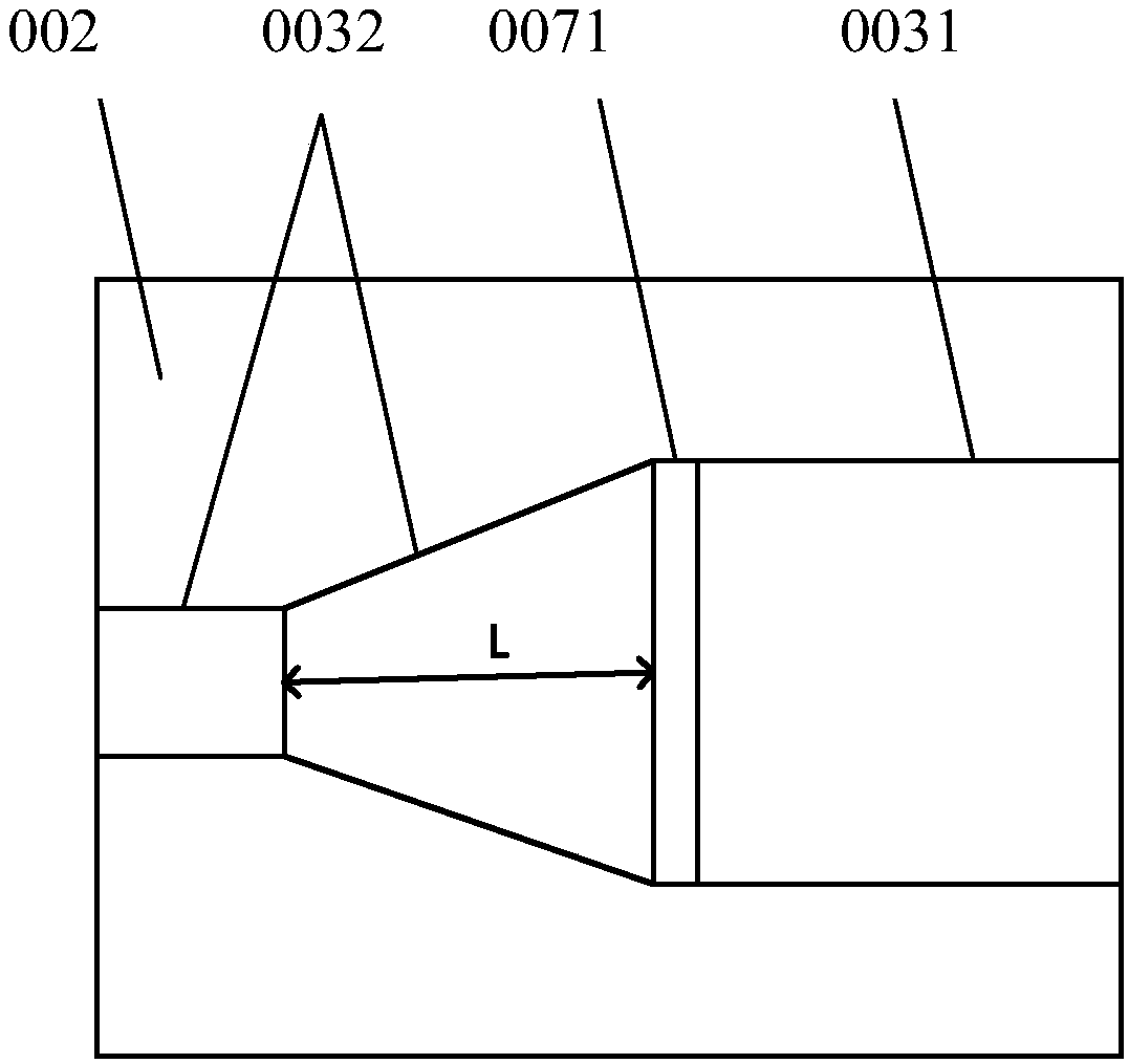
[0040] The invention relates to a Si-based modified Ge monolithic same-layer optoelectronic device. See figure 1 with figure 2 , figure 1 It is a schematic side view of the structure of a Si-based modified Ge monolithic same-layer optoelectronic device provided by an embodiment of the present invention, figure 2 It is a schematic top view of the structure of a Si-based modified Ge monolithic same-layer optoelectronic device provided by an embodiment of the present invention. Specifically, the structure includes:

[0041] P-type Si substrate layer 001;

[0042] Among them, the P-type Si substrate layer 001 has a doping concentration of 10 18 cm -3 Made of P-type Si material.

[0043] Preferably, the thickness of the P-type Si substrate layer 001 is 300-750 μm.

[0044] P-type Ge layer 002;

[0045] Among them, the P-type Ge layer 002 is located on the P-type Si substrate layer 001, and the P-type Ge layer 002 has a doping concentration of 10 20 cm -3 Made of P-type Ge material.

[0046...

Embodiment 2

[0090] See again figure 1 with figure 2 Specifically, the process flow of the Si-based modified Ge monolithic same-layer optoelectronic device includes:

[0091] Step 1. Select P-type Si substrate layer 001;

[0092] Specifically, the doping concentration is selected as 10 18 cm -3 The P-type Si substrate layer 001 with a thickness of 300-750 μm is the starting material.

[0093] Step 2. Grow a P-type Ge layer 002;

[0094] Specifically, at a temperature of 330°C, a chemical vapor deposition method was used to epitaxially grow the P-type Si substrate layer 001 with a doping concentration of 10 20 cm -3 , P-type Ge layer 002 with a thickness of 50 nm.

[0095] Step 3. Grow the intrinsic GeSn layer

[0096] Specifically, under the condition of a temperature of 350° C., an intrinsic GeSn layer with a thickness of 250 nm is grown on the P-type Ge layer 002 using a chemical vapor deposition (Chemical Vapor Deposition, CVD for short) method. By masking and ion implantation, Sn in the second ...


PUM

PropertyMeasurementUnit
thicknessaaaaaaaaaa
thicknessaaaaaaaaaa
thicknessaaaaaaaaaa

Abstract

The invention relates to a Si-based modified Ge monolithic same-layer photoelectric device. The device structurally comprises a P type Si substrate layer, a P type Ge layer arranged on the P type Si substrate layer, an intrinsic GeSn layer arranged on the P type Ge layer, a SiO2 isolation layer arranged on the P type Ge layer, an N type Ge layer arranged on a first intrinsic GeSn layer and a thirdintrinsic GeSn layer, an N type Gi layer arranged on the N type Ge layer, a SiO2 oxide layer arranged on the N type Si layer, an alpha-Si covering layer arranged on a second intrinsic GeSn layer, anda metal electrode layer arranged on the SiO2 oxide layer and the P type Ge layer. The intrinsic GeSn layer comprises a first intrinsic GeSn layer, a second intrinsic GeSn layer and a third intrinsicGeSn layer, and the second intrinsic GeSn layer is arranged between the first intrinsic GeSn layer and the third intrinsic GeSn layer. According to the invention, the light-emitting device, the waveguide and the detection device are arranged in the same layer structure on the Si-based modified Ge thin film, so that the integration level of the photoelectric device is improved, the compatibility ofthe Si substrate layer is improved, and the complexity and the cost of the preparation process of the photoelectric device are reduced.

Description

Technical field [0001] The invention belongs to the technical field of microelectronics, and specifically relates to a Si-based modified Ge monolithic same-layer optoelectronic device. Background technique [0002] With the rapid development of microelectronics technology, the integration of integrated circuits is getting higher and higher. The requirements for the switching speed of devices are becoming higher and higher. At present, the speed of electrons is basically used to the extreme, so people began to explore faster particles-photons, so optoelectronic devices came into being. [0003] At present, the development direction of optoelectronic devices is mainly divided into two aspects: one is to develop high-performance semiconductor devices through modified semiconductor materials, such as improving the performance of semiconductor devices through heterostructures; the other is to integrate different The optoelectronic device is integrated in a chip, and the integration met...

Claims


Application Information

Patent Timeline
Patent Type & Authority Applications(China)
IPC IPC(8): H01L31/153H01L31/173H01L31/18
CPCH01L31/153H01L31/173H01L31/1812Y02P70/50
Inventor 薛磊尹晓雪
Owner XIAN CREATION KEJI CO LTD
Why Eureka
Try Eureka