Layered structure capable of simultaneously realizing low laser reflection, low infrared radiation and high microwave absorption

A layered structure, low reflection technology, applied in optics, optical components, antennas, etc., can solve the problems of increased difficulty and invisible, and achieve the effect of high absorption, simple structure and small volume

Active Publication Date: 2020-07-03
INST OF OPTICS & ELECTRONICS - CHINESE ACAD OF SCI
View PDF6 Cites 24 Cited by
  • Summary
  • Abstract
  • Description
  • Claims
  • Application Information

AI Technical Summary

Problems solved by technology

To realize the invisibility of the two detection methods at the same time, it is already necessary to face many contradictions, for example: to realize the invisibility of microwave and infrared at the same time, the contradiction lies in the different performance requirements of materials in different electromagnetic wave bands; To achieve simultaneous invisibility to laser and infrared, the contradiction is that in the same electromagnetic band, materials often need to have diametrically opposite properties
However, it will be more difficult to simultaneously realize the invisibility of objects to the three detectors.

Method used


Image

  • Layered structure capable of simultaneously realizing low laser reflection, low infrared radiation and high microwave absorption
  • Layered structure capable of simultaneously realizing low laser reflection, low infrared radiation and high microwave absorption
  • Layered structure capable of simultaneously realizing low laser reflection, low infrared radiation and high microwave absorption

Examples


Embodiment 1

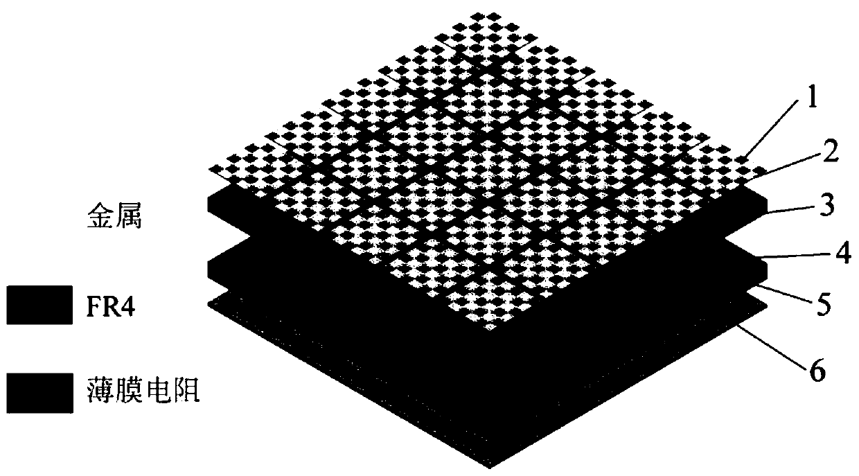
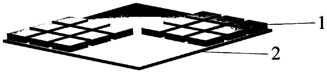
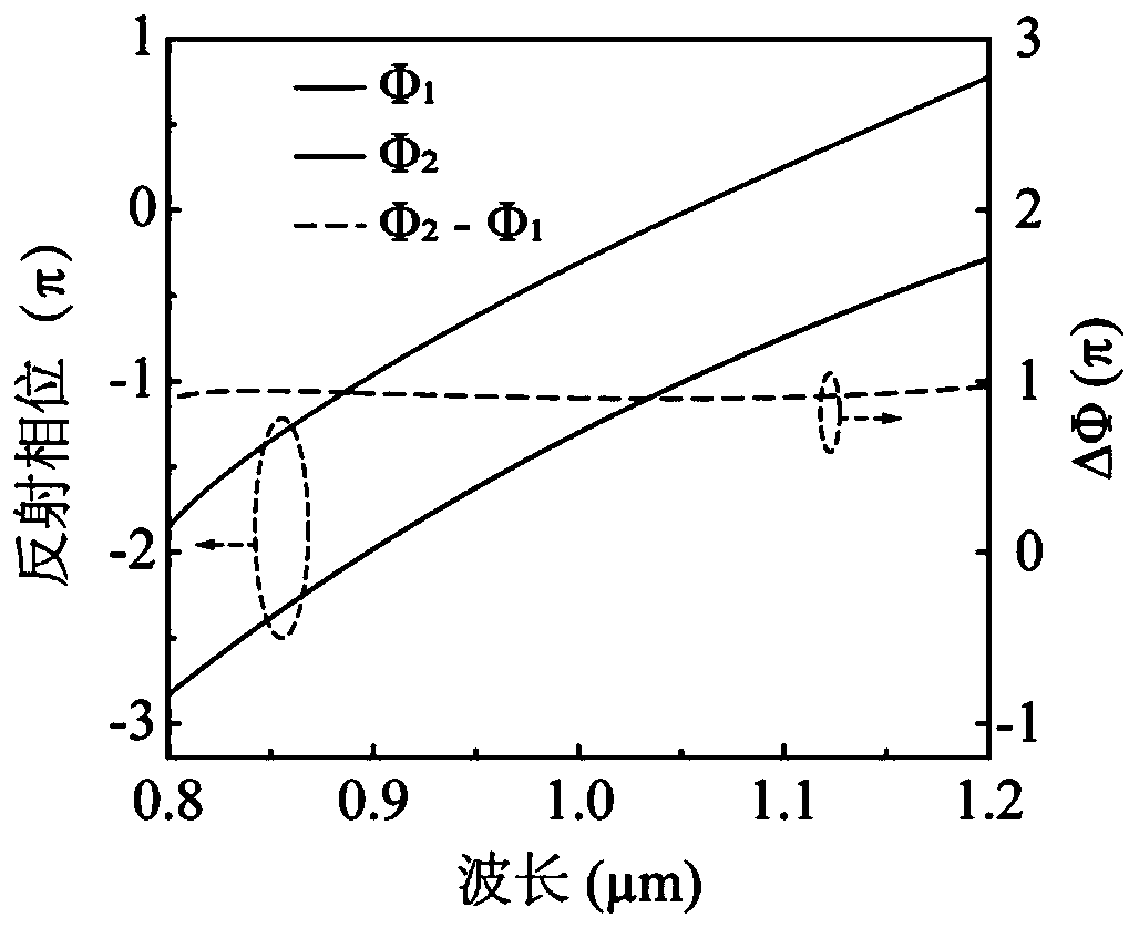
[0035] In this embodiment, a metasurface is designed for electromagnetic waves with a wavelength of 0.8-1.2 μm (center wavelength 1.06 μm). The material is selected as gold, and the dielectric constant in the corresponding wavelength band is obtained from the Palik Optical Handbook. The relevant parameters of the metasurface unit structure are Λ=0.8 μm, d=0.64 μm, h=0.22 μm. Using CST software to simulate and verify the performance of the metasurface, the simulation results are as follows image 3 , 4, 5, and 6. From image 3 It can be seen from the figure that the reflection phase difference of the two unit structures when the electromagnetic wave of 0.8-1.2 μm is irradiated is ΔΦ=π. When the two unit structures follow the figure 2 When arranged in the manner shown, a metasurface whose phase gradients in the x and y directions are both dΦ=π is obtained. Figure 4 It is shown that the metasurface is able to maintain a specular reflectance below 5% within a wide band of 0....


PUM

PropertyMeasurementUnit
heightaaaaaaaaaa
thicknessaaaaaaaaaa
thicknessaaaaaaaaaa

Abstract

The invention provides a layered structure capable of simultaneously realizing low laser reflection, low infrared radiation and high microwave absorption. The layered structure is formed by compounding an all-metal metasurface array and a metamaterial wave absorber. The all-metal metasurface array can effectively reduce specular reflectance by controlling the reflection direction of incident laser, and low laser reflection and low infrared radiation are achieved at the same time in combination with the inherent low infrared radiation characteristic of metal materials. The metamaterial wave absorber located below the all-metal metasurface array can achieve high absorption of broadband microwaves. According to the invention, the all-metal metasurface and the metamaterial wave absorber are ingeniously combined, the specular reflectance within the wave band of 0.8-1.2 microns can be effectively reduced, very low infrared emissivity is kept in infrared atmospheric windows (3-5 microns and 8-14 microns), high absorption of 6.5-13.4GHz microwaves is achieved at the same time, and multi-band electromagnetic characteristic regulation and control are achieved.

Description

technical field [0001] The invention relates to the technical field of multi-band electromagnetic wave regulation, in particular to a layered structure that realizes low laser reflection, low infrared radiation and high microwave absorption at the same time Background technique [0002] With the continuous development of multi-spectral detection technology, active detectors are often used in combination with passive detectors. For active detectors, the purpose of detection is achieved by capturing the reflected signal of the object, so the material is required to have high absorption and low reflection characteristics for electromagnetic waves. The working wavelengths of laser detection equipment mainly include 0.93 μm, 1.06 μm, 1.54 μm, and 10.6 μm, of which the two wavelengths of 1.06 μm and 10.6 μm are the most important. To achieve invisibility to passive detectors such as thermal infrared detectors, materials with low absorption and high reflectivity are required. In ...

Claims


Application Information

Patent Timeline
Patent Type & Authority Applications(China)
IPC IPC(8): G02B5/00G02B1/00H01Q15/00H01Q17/00
CPCG02B5/003G02B1/002H01Q15/0086H01Q17/00
Inventor 罗先刚马晓亮蒲明博李雄冯兴东
Owner INST OF OPTICS & ELECTRONICS - CHINESE ACAD OF SCI
Why Eureka
Try Eureka