Packaging structure, semiconductor device and packaging method

A technology of packaging structure and chip unit, applied in the direction of semiconductor devices, semiconductor/solid-state device manufacturing, semiconductor/solid-state device components, etc., can solve the problems of customer layer fracture, solder pad cracking, etc., to improve the isolation effect and stress strength. improved effect

Pending Publication Date: 2020-07-03
CHINA WAFER LEVEL CSP
View PDF0 Cites 1 Cited by
  • Summary
  • Abstract
  • Description
  • Claims
  • Application Information

AI Technical Summary

Problems solved by technology

[0004] An embodiment of the present invention provides a packaging structure, a semiconductor device and a packaging method, which are used to solve the problems in the prior art that the welding pad itself is cracked or the adjacent customer layer is broken due to the large CTE of the insulating layer, including:

Method used


Image

  • Packaging structure, semiconductor device and packaging method
  • Packaging structure, semiconductor device and packaging method
  • Packaging structure, semiconductor device and packaging method

Examples


Embodiment Construction

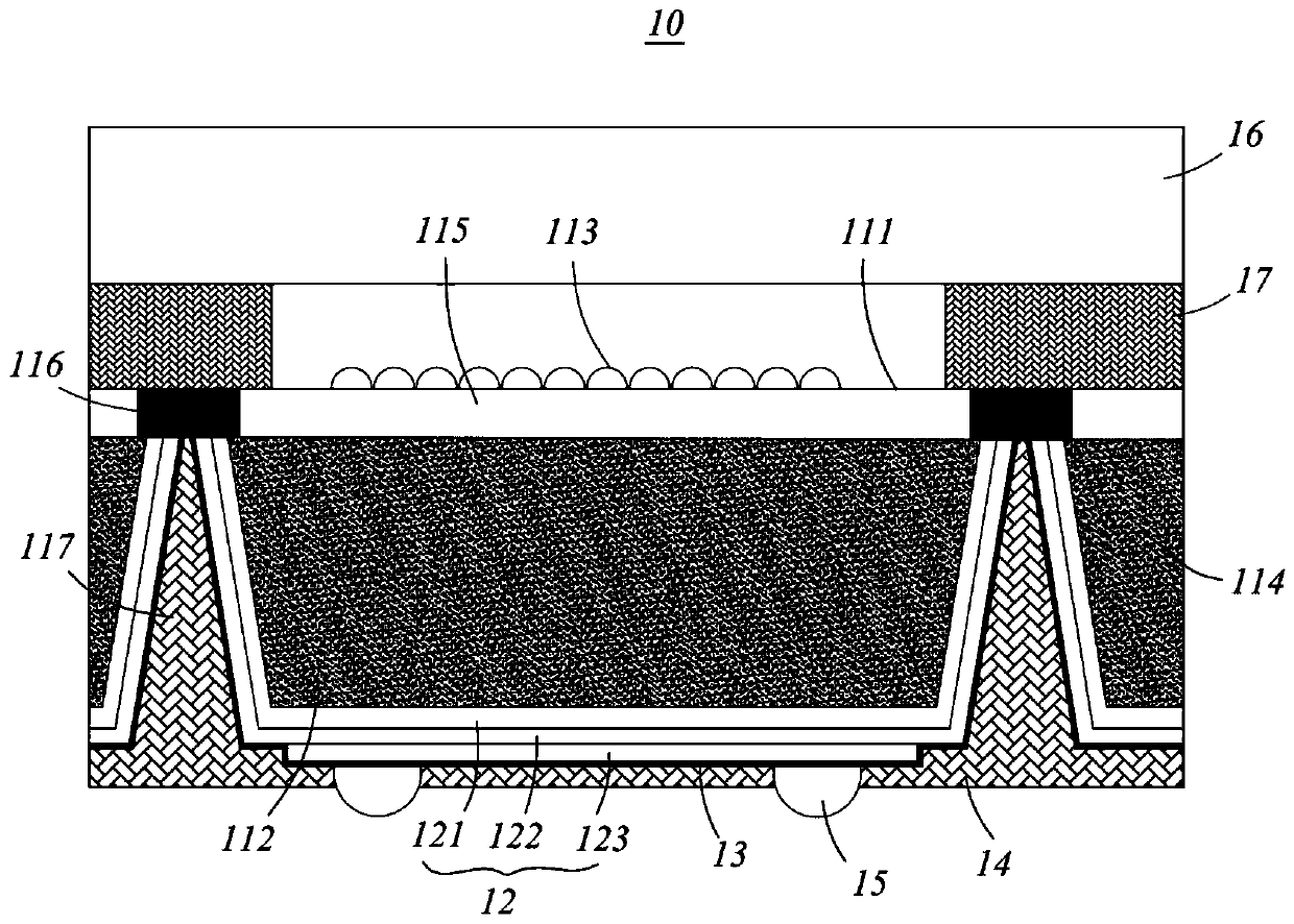
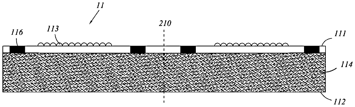
[0032] As mentioned in the background, in the existing package structure, the solder pad itself or the adjacent client layer are prone to breakage. The main reason is that in TSV (Through Silicon Via) packaging, SiO 2 Or organic materials such as epoxy resin are used as an insulating layer to cover the side walls of the through holes and connect to the pads. However, due to the large CTE (coefficient of thermal expansion) of the organic material, it is easy to pull the pads, causing the pads to break.

[0033] Aiming at the problems of the prior art, the main innovation of the embodiments of the present invention is that the insulating layer is made of SiO 2 +Si 3 N 4 + Epoxy resin three-layer structure, through this structure, the moisture insulation effect can be greatly improved, and the stress resistance strength of itself is also greatly improved, so it has a significant effect in resisting structural stress and reducing stress at the pad.

[0034] In order to make the...


PUM


Abstract

The invention discloses a packaging structure, a semiconductor device and a packaging method. The packaging structure comprises a chip unit which comprises a substrate and a client layer located on the surface of the substrate, wherein the surface, deviating from the substrate, of the client layer is defined as a first surface, the surface, deviating from the client layer, of the substrate is defined as a second surface, and a welding pad is formed in the client layer; welding bulges which are formed on the second surfaces of the chip units; a metal wiring layer which is electrically connectedbetween the welding pad and the welding bulges; and an insulating layer which is formed between the metal wiring layer and the chip unit, wherein the insulating layer comprises a silicon dioxide layer and a Si3N4 layer which are sequentially formed on the surface of the chip unit. The insulating layer of the packaging structure adopts a SiO2 + Si3N4 + epoxy resin three-layer structure, and through the structure, the moisture isolation effect can be greatly improved, and the stress resistance strength of the packaging structure is also greatly improved.

Description

technical field [0001] The invention belongs to the technical field of semiconductors, and in particular relates to a packaging structure, a semiconductor device and a packaging method, and is particularly suitable for TSV (Through Silicon Via Technology) packaging of 40nm and below Low-k (low dielectric loss constant) chips. Background technique [0002] Wafer Level Chip Size Packaging (WLCSP) technology is a technology that performs packaging and testing on the entire wafer and then cuts it to obtain a single finished chip. The size of the packaged chip is the same as that of the bare chip. Wafer-level chip packaging technology subverts traditional packaging such as ceramic leadless chip carrier (Ceramic Leadless ChipCarrier), organic leadless chip carrier (Organic Leadless ChipCarrier), and conforms to the market's increasingly light, small and short microelectronic products. , Thinning and low price requirements. The chip packaged by the wafer-level chip packaging techn...

Claims


Application Information

Patent Timeline
Patent Type & Authority Applications(China)
IPC IPC(8): H01L23/29H01L23/31H01L23/538H01L21/48H01L21/78
CPCH01L21/486H01L21/78H01L23/29H01L23/3107H01L23/5384
Inventor 王蔚钱孝清杜鹏沈戌霖
Owner CHINA WAFER LEVEL CSP
Why Eureka
Try Eureka