Supercharge Your Innovation With Domain-Expert AI Agents!

Photosensitive sensor and preparation method thereof, array substrate and display panel

A photosensitive sensor and display panel technology, applied in the semiconductor field, can solve the problems of low photoelectric response, incompatibility, affecting the accuracy of fingerprint identification, etc., and achieve the effects of increasing photocurrent, improving accuracy, and enhancing light absorption capability.

Active Publication Date: 2020-07-03
WUHAN CHINA STAR OPTOELECTRONICS TECH CO LTD
View PDF6 Cites 1 Cited by
  • Summary
  • Abstract
  • Description
  • Claims
  • Application Information

AI Technical Summary

Problems solved by technology

[0004] The manufacturing method of the existing PIN type photodiode is to realize the N-type region and the P-type region by passing through phosphine and borane during the CVD film forming process to form a diode, while the existing low temperature polysilicon (Low Temperature Poly-Silicon, LTPS for short) production line process to realize N-type or P-type transition of semiconductors is carried out by ion implantation and high temperature activation. Therefore, the existing PIN photodiode manufacturing method is not compatible with the existing LTPS production line process
For the LTPS process, due to the limitation of the polysilicon (Poly-Si) crystallization thickness by the excimer laser annealing (ELA) process, the photoelectric response of the all-Poly-Si horizontal structure PIN diode device prepared by the ion implantation process will be relatively low. Low, so that the IC cannot accurately read the signal, affecting the accuracy of fingerprint recognition

Method used


Image

  • Photosensitive sensor and preparation method thereof, array substrate and display panel
  • Photosensitive sensor and preparation method thereof, array substrate and display panel
  • Photosensitive sensor and preparation method thereof, array substrate and display panel

Examples


Embodiment Construction

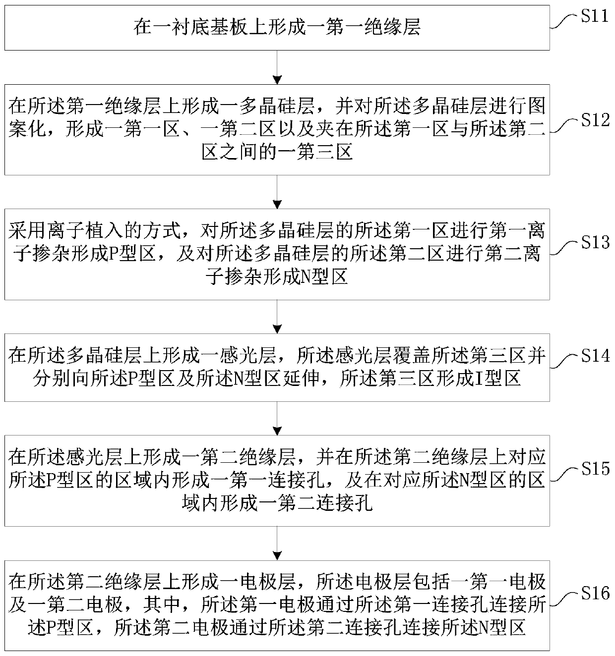
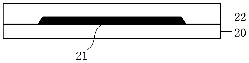
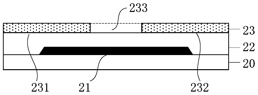
[0019] The technical solutions in the embodiments of the present application will be clearly and completely described below in conjunction with the drawings in the embodiments of the present application. Apparently, the described embodiments are only some of the embodiments of this application, not all of them. Based on the embodiments in this application, all other embodiments obtained by those skilled in the art without making creative efforts belong to the scope of protection of this application.

[0020] In the description of the present application, it should be understood that the terms "center", "longitudinal", "transverse", "length", "width", "thickness", "upper", "lower", "front", " Orientation indicated by rear, left, right, vertical, horizontal, top, bottom, inside, outside, clockwise, counterclockwise, etc. The positional relationship is based on the orientation or positional relationship shown in the drawings, which is only for the convenience of describing the a...


PUM

PropertyMeasurementUnit
thicknessaaaaaaaaaa

Abstract

The invention discloses a photosensitive sensor and a preparation method thereof, an array substrate and a display panel, an N-type region and a P-type region are respectively formed on the surface ofthe same layer of polycrystalline silicon in an ion implantation mode, and the photosensitive sensor is compatible with an ion implantation process; the amorphous silicon photosensitive layer coversthe polycrystalline silicon, so that the light absorption capability is enhanced, photo-induced electron-hole pairs can be increased, built-in electric fields exist in the horizontal direction and thevertical direction, the electron-hole pairs can be separated more effectively, the photo-induced current is increased, and the fingerprint identification precision is improved.

Description

technical field [0001] The present application relates to the technical field of semiconductors, in particular to a photosensitive sensor and a manufacturing method thereof, an array substrate, and a display panel. Background technique [0002] Fingerprints are invariable features of the human body that are inherently unique and distinguishable from others. The fingerprint pattern is unique, and it consists of a series of ridges and valleys on the surface of the fingertip skin. The fingerprint recognition technology developed from it is an earlier technology used as personal authentication. At present, fingerprint identification technology has been widely used in small and medium-sized panels, mainly including capacitive, ultrasonic and optical methods. Compared with capacitive and ultrasonic fingerprint recognition technologies, optical fingerprint recognition has good stability, strong antistatic ability, good penetration ability and low cost. Optical fingerprint recogni...

Claims


Application Information

Patent Timeline
Patent Type & Authority Applications(China)
IPC IPC(8): H01L31/105H01L31/18H01L27/32G02F1/1333G06K9/00
CPCH01L31/105H01L31/18G02F1/13338G06V40/1318H10K59/60H01L27/14678G06V40/13H01L31/035281H01L31/03762H01L27/1461H01L27/14623H01L27/14685H01L27/14692
Inventor 肖军城艾飞宋继越
Owner WUHAN CHINA STAR OPTOELECTRONICS TECH CO LTD
Features
  • R&D
  • Intellectual Property
  • Life Sciences
  • Materials
  • Tech Scout
  • Unparalleled Data Quality
  • Higher Quality Content
  • 60% Fewer Hallucinations
Learn More