Novel semiconductor crystal bar arrangement forming die

A technology for forming molds and semiconductors, which is applied in crystal growth, single crystal growth, single crystal growth, etc., and can solve problems affecting molding stability

Inactive Publication Date: 2020-07-07
朱雪玉
View PDF6 Cites 0 Cited by
  • Summary
  • Abstract
  • Description
  • Claims
  • Application Information

AI Technical Summary

Problems solved by technology

[0006] The object of the present invention is to provide a new type of semiconductor crystal rod arrangement molding die to solve the problem that when th

Method used


Image

  • Novel semiconductor crystal bar arrangement forming die
  • Novel semiconductor crystal bar arrangement forming die
  • Novel semiconductor crystal bar arrangement forming die

Examples


Embodiment Construction

[0025] The following will clearly and completely describe the technical solutions in the embodiments of the present invention with reference to the accompanying drawings in the embodiments of the present invention. Obviously, the described embodiments are only some, not all, embodiments of the present invention. Based on the embodiments of the present invention, all other embodiments obtained by persons of ordinary skill in the art without making creative efforts belong to the protection scope of the present invention.

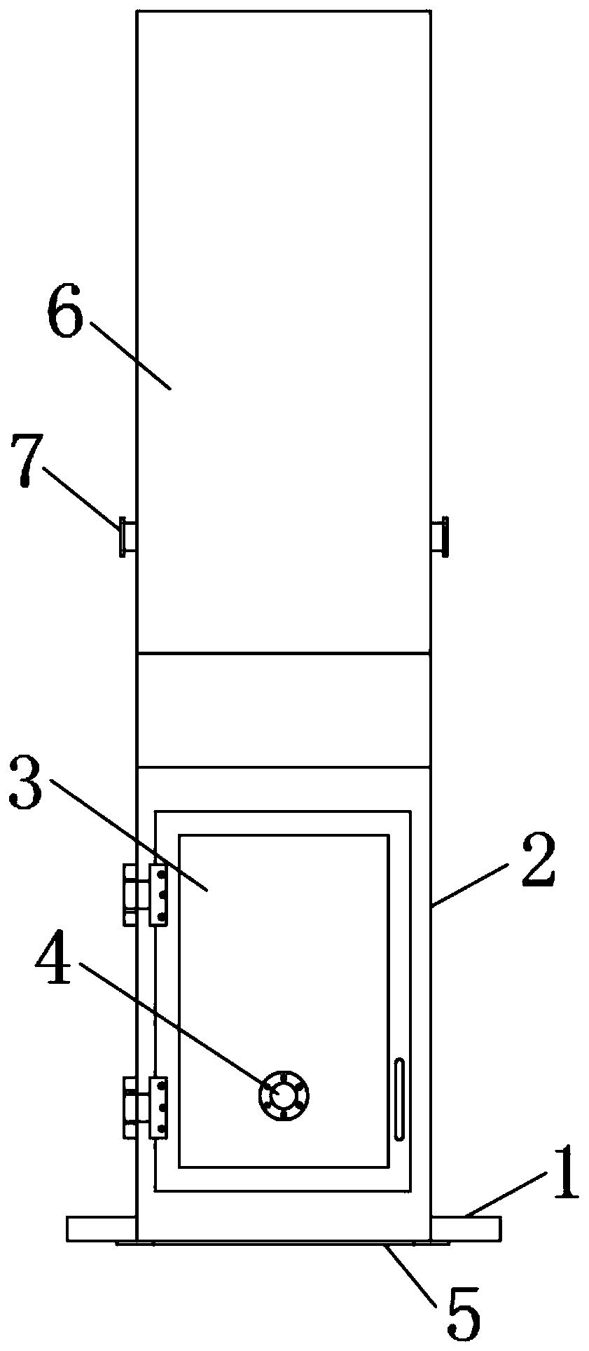
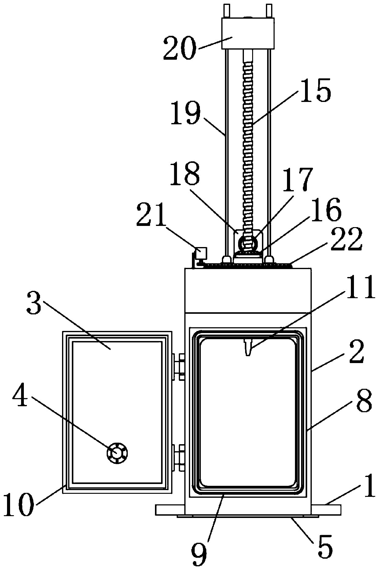
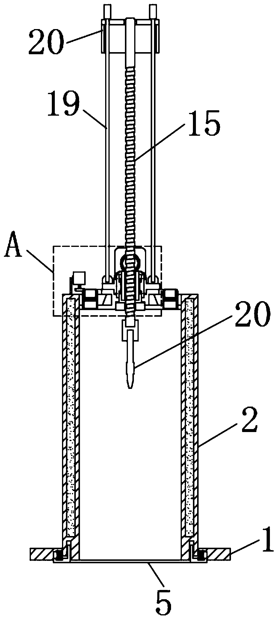
[0026] see Figure 1-7 , an embodiment provided by the present invention: a novel semiconductor crystal rod arrangement molding mold, including a base 1, a mold box 2, a seed crystal 11, a first stepping motor 18 and a second stepping motor 21, the top of the base 1 The surface is welded with mold box 2, and the front end outer surface of mold box 2 is connected with box door 3 by hinge.

[0027] The outer surface of the front end of the box door 3 is fixed w...


PUM


Abstract

The invention discloses a novel semiconductor crystal bar arrangement forming die. The die comprises a base, a mold box, a seed crystal, a first stepping motor and a second stepping motor, the mold box is welded to the upper surface of the base, and a box door is connected to the outer surface of the front end of the mold box through hinges. A protective cover is fixed to the top end of the mold box through screws. Air inlet pipes are fixed to the two sides of the protective cover through screws. A fixed seat is fixed on the upper surface of the mold box through screws; a screw sleeve is arranged on the inner side of the fixed seat in a penetrating manner; the inner side of the screw sleeve is connected with a screw sleeve through a bearing; a screw rod is arranged on the inner side of thescrew sleeve in the penetrating mode, the bottom end of the screw rod is sleeved with a permanent magnet ring, the top end of the screw sleeve is sleeved with a driven bevel gear, the outer surface of the driven bevel gear is meshed with a driving bevel gear, a guide rod is fixed to the upper surface of the fixing base, and the top end of the screw rod is sleeved with an electromagnetic disc. Thearrangement stability is improved, and the crystal bar forming yield is increased.

Description

technical field [0001] The invention relates to the technical field of semiconductor processing, in particular to a novel semiconductor crystal bar arrangement forming mold. Background technique [0002] Semiconductor ingot refers to the raw material for making silicon wafers. When the ingot is formed, it is necessary to first place blocky high-purity polycrystalline silicon in a quartz crucible and heat it to its melting point above 1420°C to completely melt it. [0003] After the temperature of the silicon melt is stable, slowly insert the seed crystal into it, then slowly lift up the seed crystal to reduce its diameter to a certain size, then maintain this diameter and elongate it by 100-200mm to eliminate the crystal seed. Due to the differences in grain arrangement and orientation within the species, after the growth of the neck is completed, slowly reduce the lifting speed and temperature, so that the diameter of the neck gradually increases to the required size, and t...

Claims


Application Information

Patent Timeline
IPC IPC(8): C30B35/00C30B29/06
CPCC30B29/06C30B35/00
Inventor 朱雪玉
Owner 朱雪玉
Why Eureka
Try Eureka