High-linearity wide-swing CMOS voltage follower

A voltage follower, high linearity technology, applied in the direction of reliability improvement modification, logic circuit connection/interface layout, logic circuit coupling/interface using field effect transistors, etc., can solve the problem of output impedance increase, super source follower The device loses the function of voltage follower, and it is difficult to expand the voltage swing, etc.

Pending Publication Date: 2020-07-07
SUZHOU UNIV
View PDF0 Cites 1 Cited by
  • Summary
  • Abstract
  • Description
  • Claims
  • Application Information

AI Technical Summary

Problems solved by technology

(3) The accompanying effect of stage (2) is that the gate voltage of the P2 tube drops, which will cause IB to enter the linear region, so r oB sharply decrease, which will lead to a sharp increase in output impedance, and the super source follower will lose its voltage following function
Compared to figure 1 , the source follower composed of IB2 and P3 tubes is added to ensure that ea...

Method used


Image

  • High-linearity wide-swing CMOS voltage follower
  • High-linearity wide-swing CMOS voltage follower
  • High-linearity wide-swing CMOS voltage follower

Examples


Embodiment

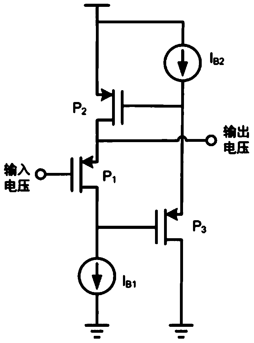
[0024] Example: refer to Figure 4 As shown, a high-linearity wide-swing CMOS voltage follower is characterized in that it includes a PMOS transistor P1, a PMOS transistor P2, a PMOS transistor P3, a PMOS transistor P4, a PMOS transistor P5, a PMOS transistor P6, a PMOS transistor P7, and a PMOS transistor. Tube P8, PMOS tube P9, PMOS tube P10, NMOS tube N1, NMOS tube N2, NMOS tube N3, NMOS tube N4, NMOS tube N5, reference current source Iref, resistor R1, resistor R2, capacitor C1, bias voltage Vb and A voltage source VDD; wherein one end of the reference current source Iref is respectively connected to one end of the resistor R1, the grid of the PMOS transistor P5, the grid of the PMOS transistor P6, the grid of the PMOS transistor P7, and the grid of the PMOS transistor P8; The other end of the resistor R1 is respectively connected to the gate of the PMOS transistor P1, the gate of the PMOS transistor P2, the gate of the PMOS transistor P3, the gate of the PMOS transistor P...

Embodiment example

[0025] The bias voltage Vb of the NMOS transistor N3 is designed at a lower value, so that the NMOS transistor N2 is biased at the edge of the saturation region. This implementation case is built under the 40nm CMOS process and 1.2V power supply voltage. The drain-source voltage of the NMOS transistor N2 is biased at about 150mV, which can ensure a more sufficient drain-source voltage of the input transistor (PMOS transistor P10), and at the same time, the PMOS transistor P10 is sufficient The drain-source voltage guarantees the better linearity performance of the present invention.

[0026] The working principle of the present invention is: the reference current is mirrored into two currents through the low-voltage cascode current mirror, and flows into the mirror image composed of NMOS transistor N1, NMOS transistor N2, NMOS transistor N4, and NMOS transistor N5 through PMOS transistor P6 and PMOS transistor P7. current source. The size ratio of NMOS transistor N4 and NMOS tr...


PUM


Abstract

The invention discloses a high-linearity wide-swing CMOS voltage follower, which has the advantages that when an input voltage is as low as 0 V, all MOS tubes can fully work in a saturation region, sothat normal operation of the voltage follower can be ensured; along with the increase of the input voltage, a drain end voltage of the PMOS tube P9 is close to a power supply voltage VDD, and the PMOS tube P9 enters a linear region, so that a grid voltage of the PMOS tube P9 is sharply reduced, but the voltage follower can still operate normally as long as the grid voltage of the PMOS tube P9 does not drop to force the NMOS tube N3 to enter the linear region. Therefore, the grid voltage of the PMOS tube P9 can be as low as 2 Vdsat, and the swing of the grid voltage of the PMOS transistor P9 is allowed to be greatly expanded.

Description

technical field [0001] The invention belongs to the technical field of integrated circuit design, in particular to a CMOS voltage follower with high linearity and wide swing. Background technique [0002] The source follower is the basic implementation of the CMOS voltage follower. A conventional super source follower circuit such as figure 1 As shown, the input terminal is the gate of the MOS transistor (high input impedance), and the output resistance is equal to Due to the negative feedback introduced by the P2 tube, the equivalent transconductance of the input tube P1 is amplified, thus providing a lower output resistance. The Thevenin equivalent model of this super source follower is as figure 2 As shown, it can be seen that its voltage gain is equal to For a voltage follower, we hope that the smaller the output resistance Rout is, the better, so that the voltage gain Av is close to 1. [0003] The power supply voltage under the advanced CMOS process has become ...

Claims


Application Information

Patent Timeline
IPC IPC(8): H03K19/003H03K19/0185
CPCH03K19/003H03K19/0185
Inventor 白春风刘天宇郭泽涛乔东海
Owner SUZHOU UNIV
Why Eureka
Try Eureka