Forming method of step structure of 3D NAND, 3D NAND memory and manufacturing method of 3D NAND memory
A 3DNAND and manufacturing method technology, applied in the direction of semiconductor devices, electrical solid devices, electrical components, etc., can solve the problems of shrinking, unfavorable device size, increasing the occupied area of the step area, etc., so as to reduce the occupied area and reduce the word line layer. Risk of short circuit, effect of size reduction
- Summary
- Abstract
- Description
- Claims
- Application Information
AI Technical Summary
Problems solved by technology
Method used
Image


Examples
Embodiment 1
[0114] This embodiment provides a method for forming a step structure of a 3D NAND memory, such as image 3 As shown, the method includes the following steps:
[0115] Step S101: providing a substrate on which a stack structure is formed, and the stack structure includes a plurality of core regions and step regions located on both sides of the core region;
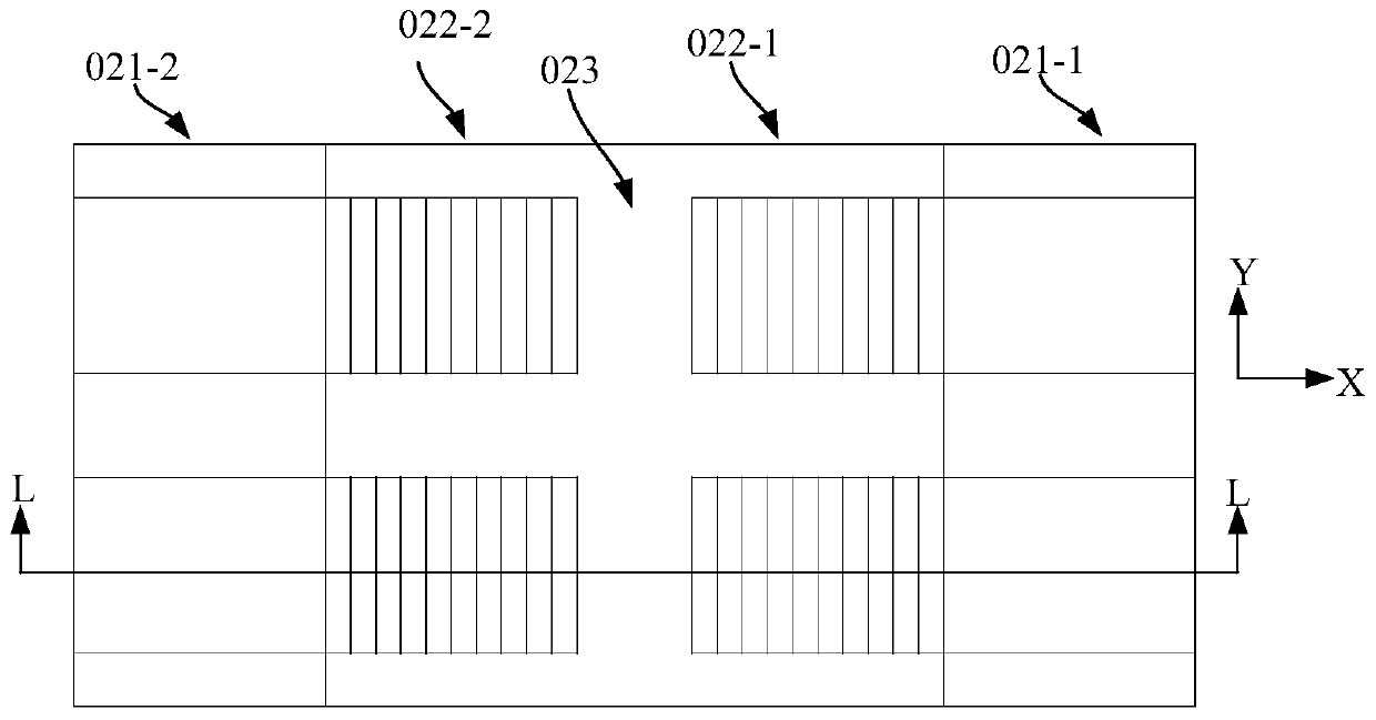
[0116] Reference Figure 4 and Figure 5 , First provide a substrate 100, the substrate 100 in the first direction namely Figure 5 The X direction and the second direction shown are Figure 5 A plane is formed in the Y direction shown. Along the third direction above the substrate 100 Figure 4 The Z direction shown forms a stacked structure 101, which is formed by alternately arranging insulating layers 1011 and sacrificial layers 1012. In this embodiment, the substrate 100 may be silicon, single crystal silicon-on-insulator or other suitable materials. The insulating layer 1011 in the stacked structure can be silicon oxide,...
Embodiment 2
[0131] This embodiment provides a 3D memory manufacturing method, such as Picture 10 As shown, the method includes the following steps:
[0132] Step S201: forming a step structure in the stacked structure of the substrate according to the method for forming the step structure described in the foregoing embodiment;
[0133] Formed according to the method described in Example 1 Figure 8 with Picture 9 For the step structure shown, the method will not be described in detail here.
[0134] Step S202: forming a storage structure in the core area;
[0135] Such as Picture 11 Shown, formed Figure 8 with Picture 9 After the stepped structure shown, the memory structure 106 is formed in the core regions 1021 and 1022.
[0136] First, like Picture 12 Shown in Picture 11 The cross-sectional view at the position shown by the center line L2-L2 is taken as an example. First, the stack structure 101 on the substrate is etched to form a channel hole 1060 penetrating the stack structure. In a ...
Embodiment 3
[0148] This embodiment provides a 3D NAND memory, which can also be referred to Figure 4 ~ Figure 9 as well as Figure 11 ~ Figure 18 , The memory includes:
[0149] A substrate; a stacked structure formed on the substrate, the stacked structure including a plurality of core regions, and step regions located on both sides of the core region; partition steps formed in the step region; formed in adjacent The first part and the second part of the partition step between the two core regions, the first part and the second part are respectively connected with two adjacent core regions; formed in the A storage structure in the core region; and a common source penetrating the stack structure, the common source penetrating the stack structure.
[0150] Reference Figure 14 ~ Figure 18 , The substrate 100 in the first direction is Figure 5 The X direction and the second direction shown are Figure 5 A plane is formed in the Y direction shown. Along the third direction above the substrate...
PUM
 Abstract
Description
Claims
Application Information
 - R&D
- Intellectual Property
- Life Sciences
- Materials
- Tech Scout
- Unparalleled Data Quality
- Higher Quality Content
- 60% Fewer Hallucinations
Browse by: Latest US Patents, China's latest patents, Technical Efficacy Thesaurus, Application Domain, Technology Topic, Popular Technical Reports.
© 2025 PatSnap. All rights reserved.Legal|Privacy policy|Modern Slavery Act Transparency Statement|Sitemap|About US| Contact US: help@patsnap.com