Light emitting diode with PIPN structure and preparation method thereof

A technology of light-emitting diodes and structural layers, which is applied to electrical components, circuits, semiconductor devices, etc., can solve the problem of excessively fast decay of light-emitting diode luminous efficiency, and achieve the effects of reducing electron transmission efficiency, reducing built-in electric field, and improving collision probability.

Active Publication Date: 2020-07-10
XIAMEN CHANGELIGHT CO LTD
View PDF5 Cites 0 Cited by
  • Summary
  • Abstract
  • Description
  • Claims
  • Application Information

AI Technical Summary

Problems solved by technology

[0005] In order to solve the above-mentioned technical problems, the present application provides a light-emitting diode with a PIPN structure and its preparation method, so as to solve the problem that the luminous efficiency of the light-emitting diode decays too quickly under high current

Method used


Image

  • Light emitting diode with PIPN structure and preparation method thereof
  • Light emitting diode with PIPN structure and preparation method thereof
  • Light emitting diode with PIPN structure and preparation method thereof

Examples


preparation example Construction

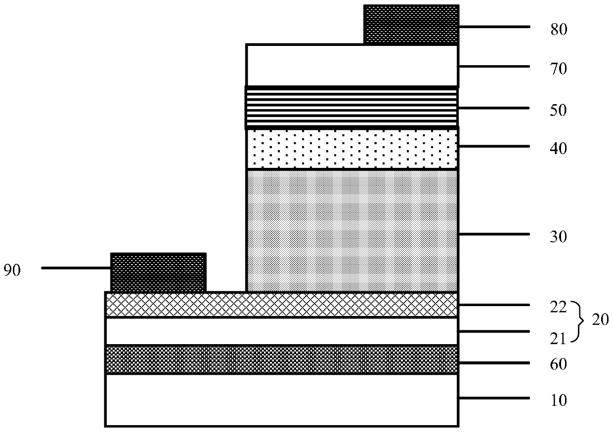
[0088] Correspondingly, the embodiment of the present application provides a method for preparing a light-emitting diode with a PIPN structure, such as Figure 4 shown, including:

[0089] S101: providing a base;

[0090] S102: sequentially forming an N-type structure layer, a P-type insertion layer, an active layer, an electron blocking layer, and a P-type hole supply layer on the surface of the substrate.

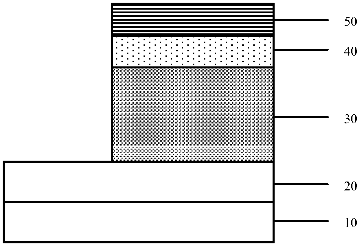
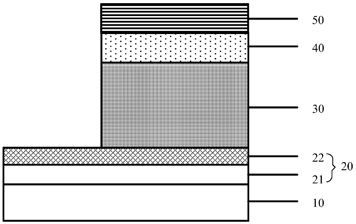
[0091] The cross-sectional structure schematic diagram of the light-emitting diode of the PIPN structure refers to figure 1 , for GaN LEDs, refer to figure 2 , optionally, the N-type structure layer includes: a U-GaN layer and an N-GaN electron supply layer; wherein,

[0092] The N-GaN electron supply layer is located on the surface of the U-GaN layer away from the substrate;

[0093] The active layer includes multiple layers of indium gallium nitride layers and multiple layers of gallium nitride layers alternately stacked;

[0094] The P-type hole supply layer incl...


PUM

PropertyMeasurementUnit
thicknessaaaaaaaaaa

Abstract

The invention discloses a light emitting diode with a PIPN structure and a preparation method thereof, a P-type insertion layer is arranged between an active layer and an N-type structure layer of thelight emitting diode, on one hand, the P-type insertion layer can be used as an electron blocking layer, and the electron transmission efficiency is reduced. On the other hand, because of existence of the P-type insertion layer, the light emitting diode is changed into a PIPN structure from an original PIN structure; a built-in electric field of the whole active layer is greatly reduced; the direction of the built-in electric field points to the P-type hole supply layer from the N-type structure layer, namely the electric field force of the built-in electric field on the holes hinders the transmission of the holes in the active layer to the N-type structure layer, so that the weakening of the built-in electric field is beneficial to improving the transmission of the holes to the N-type structure layer. Under the action of the P-type insertion layer in the two aspects, the difference of electron and hole transmission efficiency can be reduced, so that electrons and holes can be uniformly distributed in the active layer, the collision probability of the electrons and the holes is greatly improved, and the radiation recombination efficiency is further improved.

Description

technical field [0001] The present application relates to the technical field of semiconductors, and more specifically, to a light emitting diode with a PIPN structure and a preparation method thereof. Background technique [0002] A light emitting diode (Light Emitting Diode, LED), also called an electroluminescent diode, is a core component of an LED lamp. With the rapid development of light-emitting diode technology, light-emitting diodes are more and more widely used in various fields. [0003] III-V nitrides, due to their direct bandgap semiconductor characteristics, have excellent physical properties such as large forbidden band width, high breakdown electric field, and high electron saturation mobility, and have received extensive attention in the fields of electronics and optics. Among them, the blue-green light-emitting diode with GaN base as the main material has made great progress in lighting, display and digital. [0004] However, the current nitride light-emi...

Claims


Application Information

Patent Timeline
Patent Type & Authority Applications(China)
IPC IPC(8): H01L33/00H01L33/14H01L33/32
CPCH01L33/0012H01L33/0075H01L33/145H01L33/32
Inventor 卓祥景万志程伟蔺宇航尧刚
Owner XIAMEN CHANGELIGHT CO LTD
Why Eureka
Try Eureka