Structure for suppressing electromagnetic interference of circuit board and circuit board

An electromagnetic interference, circuit board technology, applied in the reduction of crosstalk/noise/electromagnetic interference (circuit devices, printed circuit components, etc., can solve the problems of increased dielectric loss, high dielectric constant, low versatility, etc.) Reduce requirements, avoid spatial conflicts, and achieve the effect of structural integration

Pending Publication Date: 2020-07-10
JIMEI UNIV
View PDF0 Cites 2 Cited by
  • Summary
  • Abstract
  • Description
  • Claims
  • Application Information

AI Technical Summary

Problems solved by technology

However, the dielectric type EBG currently being studied requires a very small interval between the power supply / ground plane, otherwise the dielectric material needs to have a high dielectric constant, and the relative dielectric constant can reach or even exceed 5000. High dielectric constant materials will cause Increased dielectric loss
Another problem with the dielectric EBG structure is that a circuit board with a certain periodic dielectric structure can only be used to suppress electromagnetic noise in a specific frequency range, and its versatility is not high.

Method used


Image

  • Structure for suppressing electromagnetic interference of circuit board and circuit board
  • Structure for suppressing electromagnetic interference of circuit board and circuit board
  • Structure for suppressing electromagnetic interference of circuit board and circuit board

Examples


Embodiment 1

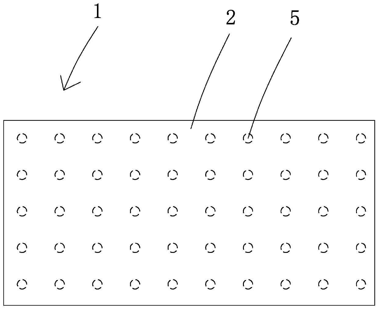
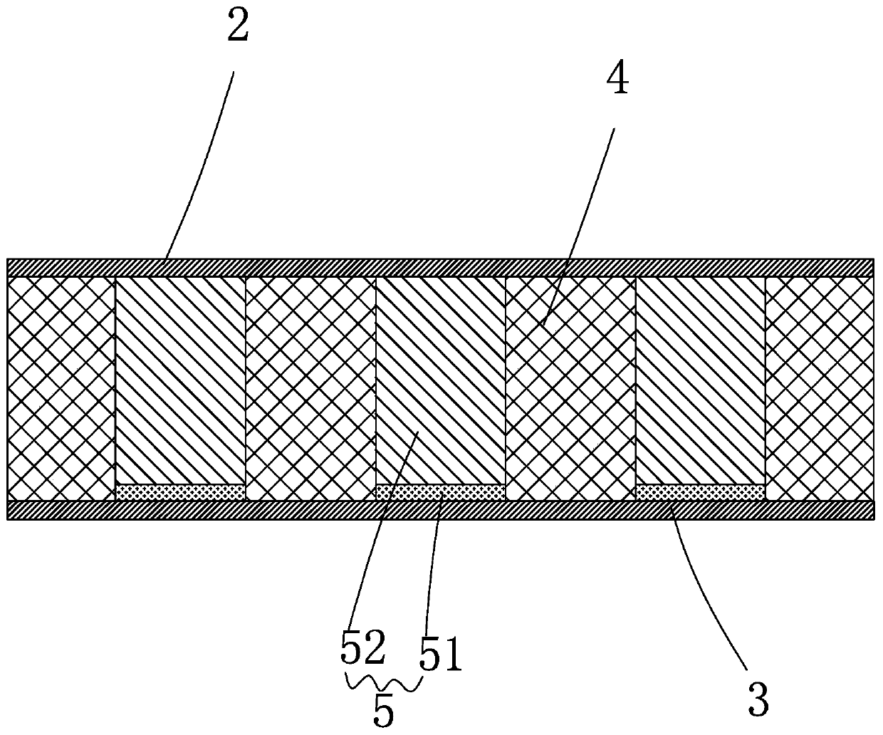
[0036] like figure 1 and 2 As shown, a circuit board electromagnetic interference suppression structure, the circuit board 1 is a multi-layer circuit board, at least includes a pair of power layer 2 and ground layer 3, between the power layer 2 and the ground layer 3 is a substrate medium 4, also includes A plurality of noise suppression units 5 embedded in the substrate medium 4 at intervals, the noise suppression units 5 are periodically distributed in the substrate medium 4, and the noise suppression units 5 include thin film units 51 with high dielectric constant and metal pillars 52, The first surface of the film unit 51 ( figure 2 The middle is the lower surface) is connected to the formation 3, the second surface of the membrane unit 51 ( figure 2 The middle is the upper surface) and the first end surface of the metal post 52 ( figure 2 The middle is the lower end surface) connection, the second end surface of the metal column 52 ( figure 2 The middle is the upp...

Embodiment 2

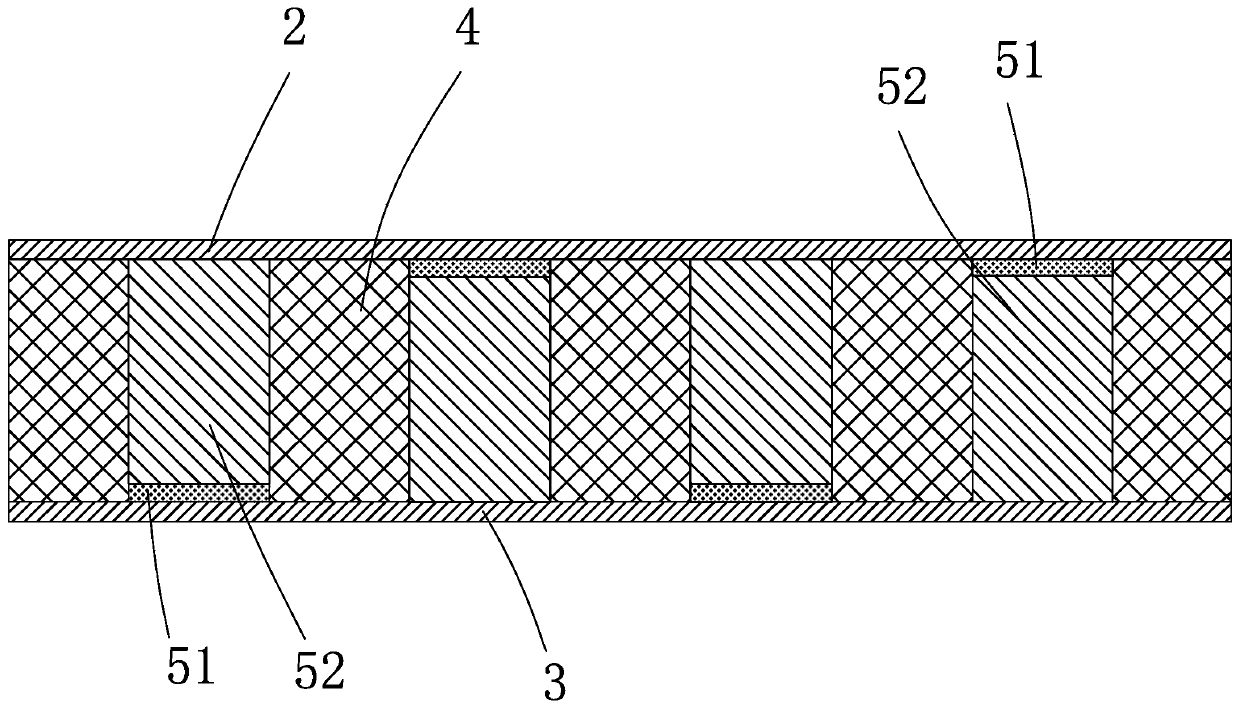
[0048] like image 3 As shown, the difference between this embodiment and Embodiment 1 is that the thin film units 51 of multiple noise suppression units 5 in this embodiment are alternately connected to the power supply layer 2 and the ground layer 3, that is, the thin film units 51 of adjacent noise suppression units 5 Arranged vertically and alternately with the metal pillars 52 , such a structure has a more complex periodic structure and is a highly nonlinear structure, which can regulate the performance of the electromagnetic structure in a wider frequency band.

Embodiment 3

[0050] like Figure 4 and 5 As shown, the difference between the present embodiment and the first embodiment is that the noise suppression unit 5 is evenly arranged around the outside of the noise source area, forming a ring structure. In this specific embodiment, the noise source area is the signal via hole 6, and the anti-pad 7 is arranged around the signal via hole 6, and a plurality of noise suppression units 5 evenly surround the anti-pad 7 to form a ring structure.

[0051] A plurality of noise suppression units 5 form a one-dimensional electromagnetic bandgap structure in cylindrical coordinates, preventing noise electromagnetic waves from propagating in the radial direction, and at the same time, the thin film unit 51 and the metal pillar 52 provide a good low-impedance return path for the return current of the signal via hole 6 , the signal integrity of the signal via hole 6 is enhanced.

[0052] Of course, in other embodiments, the noise source region may also be a...


PUM


Abstract

The invention relates to the technical field of circuit boards. The invention discloses a structure for suppressing electromagnetic interference of a circuit board. The circuit board is a multilayer circuit board, the circuit board at least comprises a pair of power layer and ground layer, and a substrate dielectric is arranged between the power layer and the ground layer. The circuit board further comprises a plurality of noise suppression units which are embedded in the substrate dielectric at intervals. The noise suppression units are periodically distributed in the substrate dielectric. Each noise suppression unit comprises a thin film unit with a high dielectric constant and a metal column, a first surface of the thin film unit is connected with the power layer or the ground layer, asecond surface of the thin film unit is connected with a first end face of the metal column, and a second end face of the metal column is connected with the ground layer or the power layer. Accordingto the invention, an enhanced dielectric EBG (electromagnetic band gap) structure is formed, the capacitance of the EBG dielectric unit is enhanced, the dielectric constant requirement of the thin film units is reduced, the electromagnetic interference suppression bandwidth is improved, and the propagation of noise electromagnetic waves between the power layer and the ground layer can be effectively suppressed.

Description

technical field [0001] The invention belongs to the technical field of circuit boards, and in particular relates to a structure for suppressing electromagnetic interference of circuit boards and a circuit board. Background technique [0002] With the rapid promotion and application of 5G technology, electronic information systems are about to enter the era of millimeter waves. The high frequency, high speed, and high density of high-speed digital systems such as integrated circuits (ICs) and high-speed printed circuit boards (PCBs) have made electromagnetic interference a problem. Very important. In high-speed multilayer PCBs, the noise sources of electromagnetic interference are extensive, among which synchronous switching noise (SSN) plays a leading role and is the main source of electromagnetic interference noise. The power distribution network (PDN) of a multilayer PCB generally adopts a planar structure, that is, a pair of adjacent power planes and ground planes. Sinc...

Claims


Application Information

Patent Timeline
Patent Type & Authority Applications(China)
IPC IPC(8): H05K1/02
CPCH05K1/0218H05K1/0231
Inventor 胡玉生
Owner JIMEI UNIV
Why Eureka
Try Eureka