MOSFET device and preparation method thereof

A device, p-type technology, applied in the field of MOSFET devices and their preparation, can solve problems such as small breakdown voltage, and achieve the effects of improving breakdown voltage, uniform electric field, and reducing electric field concentration

Pending Publication Date: 2020-07-24
SHENZHEN UNIV
View PDF5 Cites 3 Cited by
  • Summary
  • Abstract
  • Description
  • Claims
  • Application Information

AI Technical Summary

Problems solved by technology

[0004] Therefore, the technical problem to be solved in the present invention is to overcome the defect that the breakdown voltage of th

Method used


Image

  • MOSFET device and preparation method thereof
  • MOSFET device and preparation method thereof
  • MOSFET device and preparation method thereof

Examples


preparation example Construction

[0107] The embodiment of the present invention also provides a method for preparing the above-mentioned MOSFET device, including:

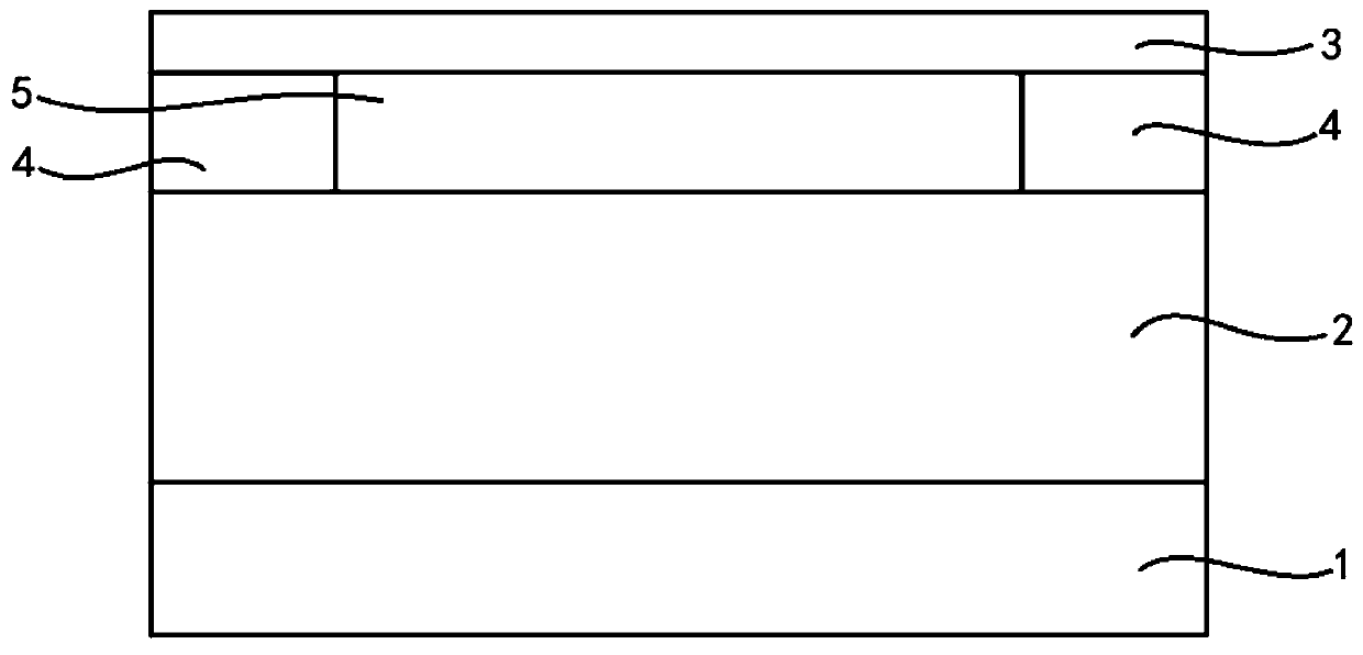
[0108] Step S1, providing a substrate 1, and sequentially forming a first n-type semiconductor layer 2, a p-type semiconductor layer and a second n-type semiconductor layer 3 on the substrate 1, the p-type semiconductor layer including a first p-type doped region 4 and the second p-type doped region 5, the first p-type doped region 4 is located on both sides of the second p-type doped region 5, and the doping concentration of the second p-type doped region 5 is higher than that of the first p-type doped region Miscellaneous area 4.

[0109] The first n-type semiconductor layer 2 and the second n-type semiconductor layer 3 are prepared by a metal organic chemical vapor deposition (MOCVD) process.

[0110] As an optional implementation, the preparation method of the p-type semiconductor layer includes:

[0111] forming a p-type semiconductor layer...

Embodiment 1

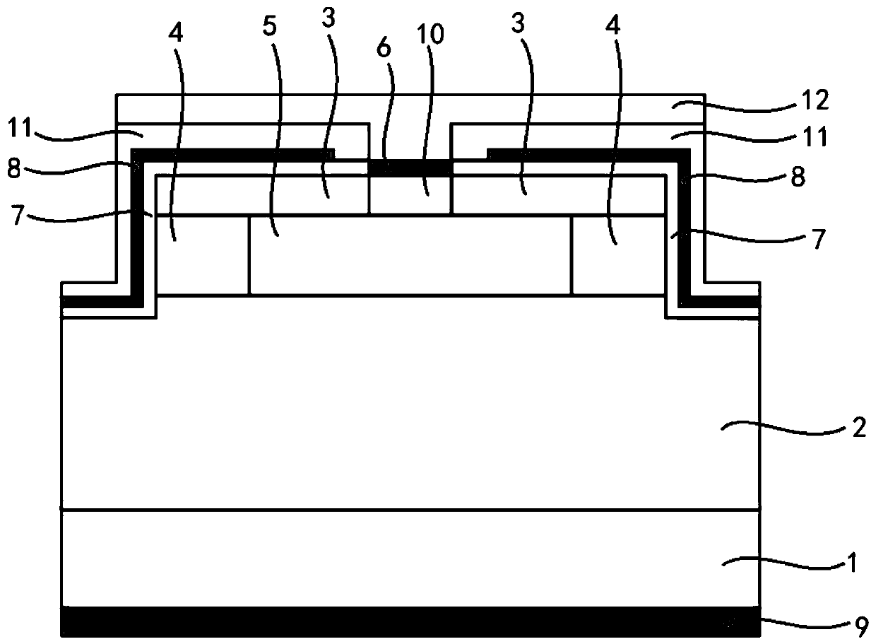
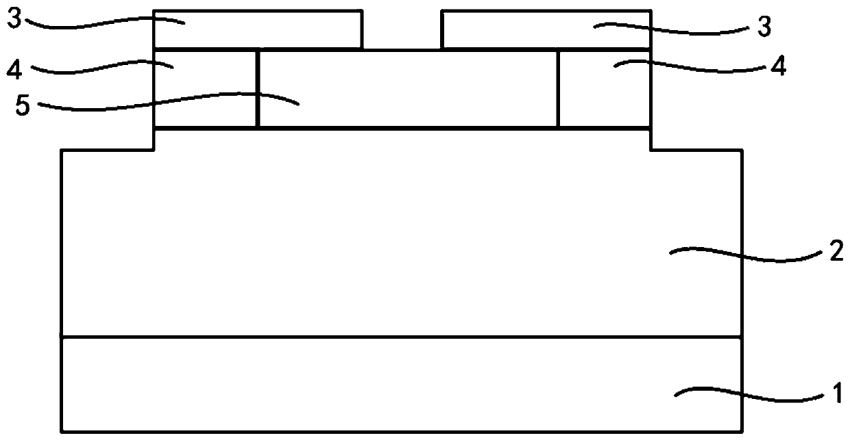
[0138] This embodiment provides a GaN-based MOSFET device, in which a drain, an n+GaN substrate, an n-GaN layer, a p-layer, and an n+GaN layer are stacked sequentially from bottom to top, wherein the p-layer consists of a p+GaN region and Composed of p-GaN regions located on the left and right sides of the p+GaN region;

[0139] A mesa structure is formed on the edge of the n-GaN layer, p layer, and n+GaN layer. The mesa structure is composed of a bottom surface and a side surface. The bottom surface is the upper surface exposed by etching the n-GaN layer, and the side surface is the n-GaN layer. , p layer, n+GaN layer is etched and exposed side;

[0140] Pd electrodes are arranged in the n+GaN layer, and the Pd electrodes are respectively in contact with the n+GaN layer and the p+GaN region;

[0141] A source is provided on the Pd electrode; a gate insulating layer is provided on the surface of the n+GaN layer located on the left and right sides of the source and extends to ...

Embodiment 2

[0158] This embodiment provides a method for preparing a GaN-based MOSFET device in Embodiment 1, and the steps are as follows:

[0159] (1) Prepare a commercially available n+GaN substrate;

[0160](2) The n-GaN layer and the p-layer are sequentially grown on the n+GaN substrate by a metal organic chemical vapor deposition (MOCVD) process;

[0161] (3) Use an ion implanter to implant p-type dopants in the middle of the p-layer at a distance of 5 μm from the left and right ends to form a p+GaN region, and p-GaN regions are formed on both sides;

[0162] (4) growing an n+GaN layer on the p layer by metal organic chemical vapor deposition (MOCVD);

[0163] (5) Using inductively coupled plasma etching (ICP), using Cl 2 / SiCl 4 Dry etching etches a mesa structure on the left and right edges of the n-GaN layer, p layer, and n+GaN layer, and etches a groove in the middle of the n+GaN layer;

[0164] (6) A magnetron sputtering process is used to form a Pd electrode in the groove;...


PUM

PropertyMeasurementUnit
Widthaaaaaaaaaa
Side heightaaaaaaaaaa
Thicknessaaaaaaaaaa

Abstract

The invention provides an MOSFET device and a preparation method thereof. The MOSFET device comprises a substrate; a first n-type semiconductor layer, a p-type semiconductor layer and a second n-typesemiconductor layer are sequentially stacked on the substrate; the p-type semiconductor layer comprises a first p-type doped region and a second p-type doped region; the first p-type doped region is located on the two sides of the second p-type doped region, and the doping concentration of the second p-type doped region is higher than that of the first p-type doped region; the MOSFET device further comprises a source electrode which is arranged on the side, deviating from the p-type semiconductor layer, of the second n-type semiconductor layer and makes contact with the second n-type semiconductor layer and the second p-type doped region, a gate insulating layer and a gate; the gate insulating layer and the gate are sequentially stacked on the exposed surfaces of the second n-type semiconductor layer, the p-type semiconductor layer and the first n-type semiconductor layer; the MOSFET device further comprises a drain electrode which is arranged on one side, deviating from the first n-type semiconductor layer, of the substrate. A step-doped p region is formed on the p-type semiconductor layer, so that the breakdown voltage of the device is improved. The process is simple, and preparation is convenient.

Description

technical field [0001] The invention relates to the technical field of semiconductor devices, and more particularly relates to a MOSFET device and a preparation method thereof. Background technique [0002] Metal-Oxide-Semiconductor Field-Effect Transistor (MOSFET) is a field-effect transistor (field-effect transistor) that can be widely used in analog circuits and digital circuits. MOSFET is a device that controls the drain current through the gate-source voltage. Specifically, when a sufficiently large potential difference is applied between the gate and source of the MOSFET, the electric field will be under the oxide layer The induced charge is formed on the surface of the semiconductor, and at this time the so-called "inversion channel" will be formed. The polarity of the channel is the same as that of the drain and the source. After the channel is formed, the MOSFET can Let the current flow, and according to the voltage value applied to the gate, the magnitude of the c...

Claims


Application Information

Patent Timeline
IPC IPC(8): H01L29/06H01L29/40H01L29/41H01L29/423H01L29/78H01L21/336H01L21/28
CPCH01L29/7827H01L29/66666H01L29/0684H01L29/0619H01L29/0623H01L29/42356H01L29/0611H01L29/402H01L29/66522H01L29/401H01L29/41
Inventor 刘新科利健陈勇林峰王磊罗江流贺威
Owner SHENZHEN UNIV
Why Eureka
Try Eureka