
Semiconductor device structure and manufacturing method thereof

A technology of device structure and manufacturing method, which is applied in the direction of semiconductor devices, semiconductor/solid-state device manufacturing, and electric solid-state devices, can solve the problems of only discrete channel width changes, layout loss, and reduced circuit integration, and achieve improved The effect of device integration and device performance, reducing interface traps and improving reliability

Inactive Publication Date: 2020-07-24
SIEN QINGDAO INTEGRATED CIRCUITS CO LTD
View PDF0 Cites 0 Cited by
  • Summary
  • Abstract
  • Description
  • Claims
  • Application Information

AI Technical Summary

Problems solved by technology

[0005] FinFET devices are usually fabricated based on fin-shaped semiconductor layers on a substrate. However, generally all fin-shaped semiconductor layers on a substrate have the same height. For this reason, the channel width of a FinFET device Limited by this height, the channel width can only be changed discretely, not continuously, which greatly reduces the flexibility of circuit design.
In addition, compared with planar gate type devices (planar gate type devices can continuously adjust their channel width), FinFET devices may cause certain layout due to design limitations (cannot continuously adjust channel width). loss, resulting in a reduction in circuit integration

Method used


Image

  • Semiconductor device structure and manufacturing method thereof
  • Semiconductor device structure and manufacturing method thereof
  • Semiconductor device structure and manufacturing method thereof

Examples


Embodiment 1

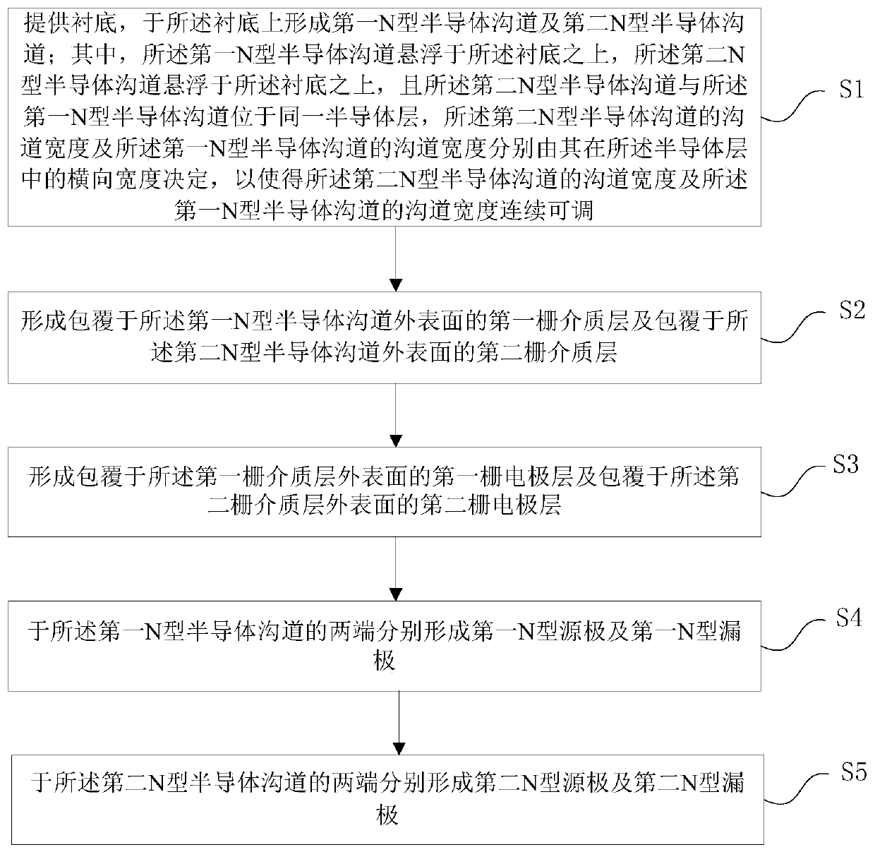
[0083] see figure 1 , the invention provides a method for manufacturing a semiconductor device structure, the method for manufacturing a semiconductor device structure includes the steps of:

[0084] 1) Provide a substrate, and form a first N-type semiconductor channel and a second N-type semiconductor channel on the substrate; wherein, the first N-type semiconductor channel is suspended above the substrate, and the The second N-type semiconductor channel is suspended above the substrate, and the second N-type semiconductor channel is located in the same semiconductor layer as the first N-type semiconductor channel, and the second N-type semiconductor channel The channel width of the channel and the channel width of the first N-type semiconductor channel are respectively determined by its lateral width in the semiconductor layer, so that the channel width of the second N-type semiconductor channel and the The channel width of the first N-type semiconductor channel is continuo...

Embodiment 2

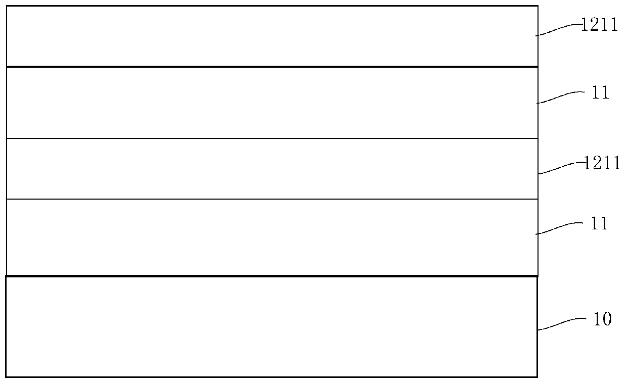
[0127] Please combine Figure 2 to Figure 11 read on Figure 12 , the present invention also provides a semiconductor device structure, the semiconductor device structure includes: a substrate 10; a first N-type semiconductor channel 121, the first semiconductor channel 121 is suspended above the substrate 10; Two N-type semiconductor channels 131, the second N-type semiconductor channel 131 is suspended above the substrate 10, the second N-type semiconductor channel 131 and the first N-type semiconductor channel 121 are located In the same semiconductor layer, the channel width of the second N-type semiconductor channel 131 and the channel width of the first N-type semiconductor channel 121 are respectively determined by their lateral widths in the semiconductor layer, so that the The channel width of the second N-type semiconductor channel 131 and the channel width of the first N-type semiconductor channel 121 are continuously adjustable; the first gate dielectric layer 122...


PUM

PropertyMeasurementUnit
thicknessaaaaaaaaaa
thicknessaaaaaaaaaa

Abstract

The invention provides a semiconductor device structure and a manufacturing method thereof. The semiconductor device structure comprises a substrate, a first N-type semiconductor channel, and a secondN-type semiconductor channel. The channel width of the second N-type semiconductor channel and the channel width of the first N-type semiconductor channel are respectively determined by the transverse width of the second N-type semiconductor channel and the transverse width of the first N-type semiconductor channel in a semiconductor layer, so that the channel width of the second N-type semiconductor channel and the channel width of the first N-type semiconductor channel are continuously adjustable. The semiconductor device structure further comprises a first gate dielectric layer, a firstgate electrode layer, a first N-type source electrode, a first N-type drain electrode, a second gate dielectric layer, a second gate electrode layer, a second N-type source electrode and a second N-type drain electrode. According to the invention, the width of the second N-type semiconductor channel and the channel width of the first N-type semiconductor channel can be continuously adjusted; the design flexibility of a semiconductor memory device can be greatly improved; and the integration level and the performance of the device are improved.

Description

technical field [0001] The invention belongs to the technical field of integrated circuit design and manufacture, and in particular relates to a semiconductor device structure and a manufacturing method thereof. Background technique [0002] With the continuous development of semiconductor technology, the size of semiconductor devices is continuously reduced, the performance of driving current is continuously improved, and the power consumption is continuously reduced. production cost. [0003] Fin Field-Effect Transistor (FinFET) is a new complementary metal oxide semiconductor transistor. The shape of FinFET is similar to that of a fish fin. This design can improve circuit control and reduce leakage current, shortening the gate length of transistors. [0004] FinFET is an innovative design derived from the traditional standard transistor—Field-Effect Transistor (FET). In the traditional transistor structure, the gate can only control the on and off of the current on one...

Claims


Application Information

Patent Timeline
Patent Type & Authority Applications(China)
IPC IPC(8): H01L29/10H01L29/78H01L27/11H01L21/8244H01L21/336H10B10/00
CPCH01L29/785H01L29/66795H01L29/1054H10B99/00H10B10/12
Inventor 肖德元
Owner SIEN QINGDAO INTEGRATED CIRCUITS CO LTD
Learn More