Inverted light emitting diode
A light-emitting diode, flip-chip technology, applied in electrical components, circuits, semiconductor devices, etc., can solve the problems of uneven coverage of the insulating protective layer, short circuit, cracking of the insulating protective layer, etc., to improve long-term reliability and technical application range. Wide and small effect of brightness
- Summary
- Abstract
- Description
- Claims
- Application Information
AI Technical Summary
Problems solved by technology
Method used
Image

Examples
Embodiment 2
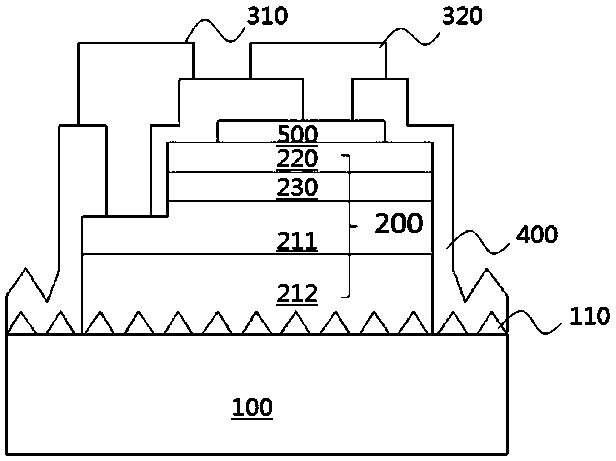
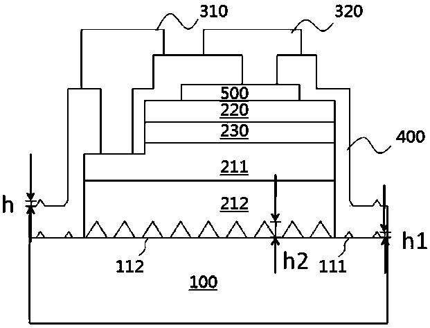
[0057] refer to Figure 6 According to the light-emitting diode of the third embodiment listed in the present invention, the process of reducing the size of the protrusions and expanding the distribution density of the protrusions on the substrate is adopted. Compared with the second embodiment of the present invention, the manufacturing process of this embodiment is operable Higher, one of the methods for making the substrate is to change the mask pattern and adjust the etching time when making the pattern substrate to make a raised pattern with a predetermined size and suitable density. This process has been established in the substrate industry. Mature technology, no more details here. In the chip structure of this embodiment, the height of the protrusions 111 in the area covered by the first semiconductor layer of the substrate 100 is 1 to 2 microns, and it can also be said that the height of the protrusions of the entire substrate 100 is 1 microns to 2 microns, while The...
PUM
| Property | Measurement | Unit |
|---|---|---|
| Length | aaaaa | aaaaa |
| Width | aaaaa | aaaaa |
| Height | aaaaa | aaaaa |
Abstract
Description
Claims
Application Information
 - Generate Ideas
- Intellectual Property
- Life Sciences
- Materials
- Tech Scout
- Unparalleled Data Quality
- Higher Quality Content
- 60% Fewer Hallucinations
Browse by: Latest US Patents, China's latest patents, Technical Efficacy Thesaurus, Application Domain, Technology Topic, Popular Technical Reports.
© 2025 PatSnap. All rights reserved.Legal|Privacy policy|Modern Slavery Act Transparency Statement|Sitemap|About US| Contact US: help@patsnap.com