Strong heat dissipation structure capable of being used for heat dissipation of optoelectronic device and preparation method of structure

A technology for optoelectronic devices and heat dissipation structures, which is applied in the fields of electro-solid devices, semiconductor/solid-state device manufacturing, and electrical components. , Improve heat dissipation efficiency and effectively conduct heat

Pending Publication Date: 2020-08-04
UNIV OF ELECTRONIC SCI & TECH OF CHINA
View PDF5 Cites 1 Cited by
  • Summary
  • Abstract
  • Description
  • Claims
  • Application Information

AI Technical Summary

Problems solved by technology

However, the traditional preparation process of graphene-based heat dissipation film is mainly made by direct calendering after graphite treatment and polymer carbonization and graphitization. This method is limited by the planar structure of the material itself on the thermal conductivity and graphite Due to the limitation of the preparation process of olefin film, the size of the prepared graphite film is within tens of centimeters, which is unacceptable for highly integrated optoelectronic devices or flexible devices with high output power and high heat dissipation requirements.
At the same time, the graphene film is easily broken locally and the edge of the film is easily damaged during the preparation process, which will easily lead to uneven local heat dissipation and poor product repeatability, which will not only increase the cost of optoelectronic products Reduce product yield and device efficiency
In addition, graphene heat dissipation materials are not flexible and fragile, which seriously restricts the application of graphene and graphene oxide films in industrialization.

Method used


Image

  • Strong heat dissipation structure capable of being used for heat dissipation of optoelectronic device and preparation method of structure

Examples


Embodiment 1

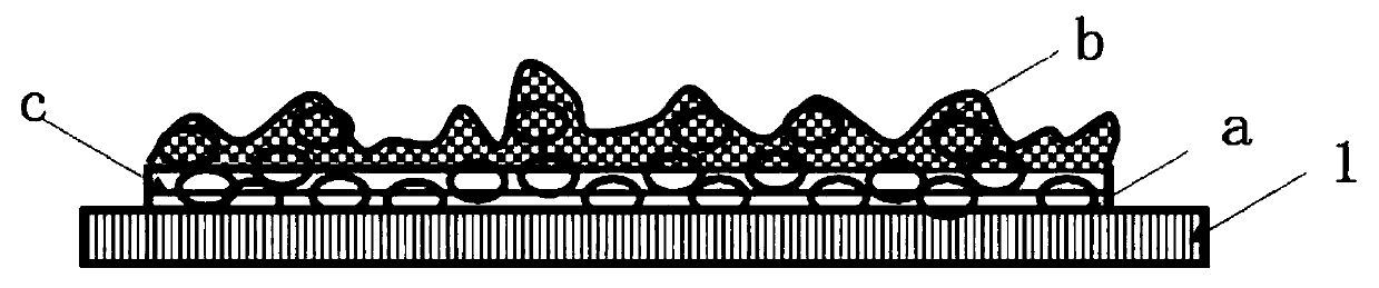
[0030] like figure 1 As shown, this embodiment provides a strong heat dissipation structure that can be used for heat dissipation of optoelectronic devices, including a bottom-up base 1 and a strong heat dissipation film. The total thickness of the strong heat dissipation film is 15 μm, and the raw materials of the strong heat dissipation film are as follows: The weight ratio includes the following components: 50% heat absorbing agent, 10% intermediate connecting agent, 35% cooling agent, and 5% protecting agent;

[0031] The heat-absorbing agent is silver nanospheres, the intermediate connecting agent is a single-layer two-dimensional MoS2 film, the cooling agent is silver nanowires, and the protective agent is a mixture of Schima trunk and leaf extract containing 5% polyether-modified polysiloxane.

[0032] The preparation method is as follows:

[0033] Step 1. First, clean the radiator or the substrate 1 on the surface to be sprayed, and perform ultrasonic cleaning with de...

Embodiment 2

[0042] like figure 1 As shown, this embodiment provides a strong heat dissipation structure that can be used for heat dissipation of optoelectronic devices, including a bottom-up base 1 and a strong heat dissipation film. The total thickness of the strong heat dissipation film is 15 μm, and the raw materials of the strong heat dissipation film are as follows: The weight ratio includes the following components: 45% heat absorbing agent, 15% intermediate connecting agent, 35% cooling agent, and 5% protecting agent;

[0043] The heat-absorbing agent is silver nanospheres, the intermediate connecting agent is a single-layer two-dimensional MoS2 film, the cooling agent is silver nanowires, and the protective agent is a mixture of Schima trunk and leaf extract containing 5% polyether-modified polysiloxane.

[0044] The preparation method is as follows:

[0045] Step 1. First, clean the radiator or the substrate 1 on the surface to be sprayed, and perform ultrasonic cleaning with de...

Embodiment 3

[0054] like figure 1 As shown, this embodiment provides a strong heat dissipation structure that can be used for heat dissipation of optoelectronic devices, including a bottom-up base 1 and a strong heat dissipation film. The total thickness of the strong heat dissipation film is 15 μm, and the raw materials of the strong heat dissipation film are as follows: The weight ratio includes the following components: 45% heat absorbing agent, 20% intermediate connecting agent, 30% cooling agent, and 5% protecting agent;

[0055] The heat-absorbing agent is silver nanospheres, the intermediate connecting agent is a single-layer two-dimensional MoS2 film, the cooling agent is silver nanowires, and the protective agent is a mixture of Schima trunk and leaf extract containing 5% polyether-modified polysiloxane.

[0056] The preparation method is as follows:

[0057] Step 1. First, clean the radiator or the substrate 1 on the surface to be sprayed, and perform ultrasonic cleaning with de...


PUM

PropertyMeasurementUnit
Thicknessaaaaaaaaaa
Thicknessaaaaaaaaaa

Abstract

The invention discloses a strong heat dissipation structure capable of being used for heat dissipation of an optoelectronic device and a preparation method of the strong heat dissipation structure, and relates to the technical field of heat dissipation materials. The material comprises a substrate and a strong heat dissipation thin film from bottom to top, the total thickness of the strong heat dissipation thin film does not exceed 15 microns, and the strong heat dissipation thin film comprises the following raw materials in percentage by weight: 50 to 30 percent of a heat absorbent, 10 to 20percent of an intermediate coupling agent, 35 to 45 percent of a heat dissipation agent and 5 percent of a protective agent. The structure and method are used for heat dissipation of the optoelectronic device, the high-heat-dissipation thin film has a large specific surface area and high heat conductivity, and the heat dissipation efficiency can be effectively improved.

Description

technical field [0001] The invention relates to the technical field of potato production, in particular to a strong heat dissipation structure which can be used for heat dissipation of optoelectronic devices and a preparation method thereof. Background technique [0002] Today's society requires optoelectronic equipment to be light in weight, easy to carry, flexible and transparent, and increasingly integrated, making various optoelectronic products develop rapidly in the direction of thin, light, and small, which is very easy to cause optoelectronics. Product surface temperature rises. Since optoelectronic devices need a relatively low temperature environment to operate reliably, in order to improve the service life of various components inside optoelectronic devices, the heat dissipation of electronic products has become a very prominent problem. In particular, there is a common problem in all kinds of optoelectronic devices at present, that is, the problem of heat dissip...

Claims


Application Information

Patent Timeline
IPC IPC(8): H01L23/373H01L21/48
CPCH01L23/3735H01L21/4803
Inventor 于军胜周殿力杨根杰高林
Owner UNIV OF ELECTRONIC SCI & TECH OF CHINA
Why Eureka
Try Eureka