P-surface metal preparation method of ridge-type GaAs-based laser with deep groove

A laser, deep trench technology, applied in lasers, laser parts, semiconductor lasers, etc., can solve problems such as caps, difficult to meet, different corrosion rates, etc., to prevent metal faults, shorten production cycles, and reduce consumption.

Active Publication Date: 2020-08-04
潍坊华光光电子有限公司
View PDF8 Cites 2 Cited by
  • Summary
  • Abstract
  • Description
  • Claims
  • Application Information

AI Technical Summary

Problems solved by technology

[0004] Moreover, due to the needs of product upgrading, many products currently need to etch relatively deep grooves on the surface of the chip, some of which have reached more than 4um. Moreover, due to the differences in the materials of each part of the epitaxial layer, in the process of wet etching , the corrosion rate of various materials is different, and it is easy to cause the capping phenomenon of the ridge top area during the corrosion process
The above two methods are difficult to meet the needs of the P-side metal layer of the ridge waveguide structure with deep grooves

Method used


Image

  • P-surface metal preparation method of ridge-type GaAs-based laser with deep groove
  • P-surface metal preparation method of ridge-type GaAs-based laser with deep groove
  • P-surface metal preparation method of ridge-type GaAs-based laser with deep groove

Examples


preparation example Construction

[0031] A method for preparing a P-face metal of a ridge-type GaAs-based laser with deep grooves, comprising the steps of:

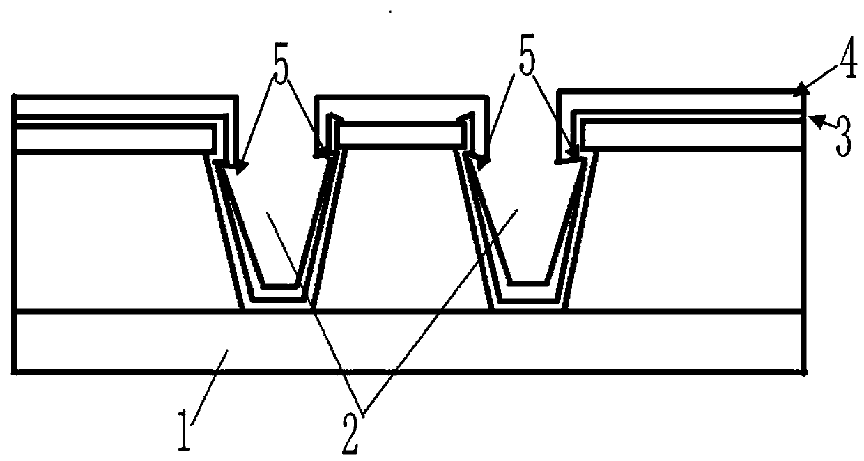
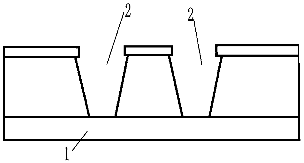
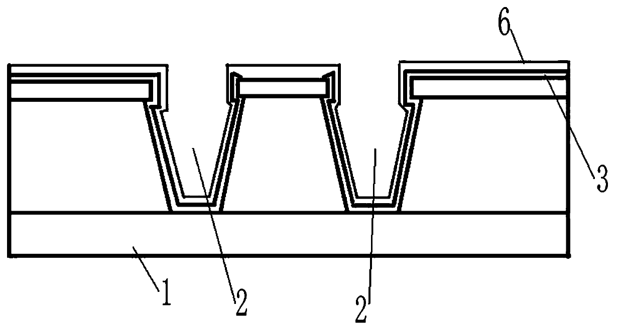
[0032] a) Prepare the epitaxial wafer 1. The epitaxial wafer includes substrate, N confinement layer, quantum well active area, AlGaInP layer and GaAs layer from bottom to top, and etches a ridge-shaped light-emitting area on the AlGaInP layer and GaAs layer, and the ridge-shaped light-emitting area Ridge grooves 2 are formed on both sides of the region;

[0033] b) preparing a layer of silicon dioxide passivation film 3 on the surface of the epitaxial wafer 1 other than the ridge-shaped light-emitting region using PECVD equipment and photolithography;

[0034] c) Spin-coat a layer of negative photoresist on the silicon dioxide passivation film 3, and prepare a P electrode pattern by photolithography and development;

[0035] d) growing a metal layer 6 on the silicon dioxide passivation film 3 according to the region of the P electrode pattern, the metal...

Embodiment 1

[0042] The depth of the ridge groove 2 in step a) is greater than 2 μm and less than 8 μm.

Embodiment 2

[0044] The thickness of the silicon dioxide passivation film 3 in step b) is 1000-2000 angstroms.


PUM

PropertyMeasurementUnit
depthaaaaaaaaaa
thicknessaaaaaaaaaa
thicknessaaaaaaaaaa

Abstract

The invention discloses a P-surface metal preparation method of a ridge-type GaAs-based laser with a deep groove. The method is characterized by coating negative photoresist on a silicon dioxide passive film, roughening an Au layer at the uppermost end in a metal layer on the negative photoresist, and preparing an Au conducting layer after roughening treatment, so that the covering stability of the Au conducting layer can be improved; the preparation rate of the metal layer is relatively low, the growth rates of the Au conducting layer from the first Au layer to the fourth Au layer are sequentially increased, vapor deposition of a P-surface metal layer composed of the metal layer and the Au conducting layer of the ridge waveguide structure laser with the groove depth larger than 2 micronscan be completed through different growth rates, so that P-surface polymer filling and leveling-up are avoided, and metal faults are prevented; operation is convenient, the process steps are simplified, and the production period is shortened; and meanwhile, consumption of raw materials is reduced, and repeatability and stability of the whole process are improved.

Description

technical field [0001] The invention relates to the technical field of manufacturing semiconductor lasers, in particular to a P-plane metal preparation method of a ridge-type GaAs-based laser with deep grooves. Background technique [0002] Since the advent of semiconductor lasers, due to their advantages such as small size, high power, long life, and convenient use, they have been favored in the fields of optical storage, optical communications, national defense, and medical treatment. Due to the impact of product production process implementation and product performance, as shown in Figure 1, most of the current semiconductor lasers use a ridge waveguide structure, that is, the current injection area of ​​the ridge is relatively high, and the two sides of the ridge groove 2 It is necessary to etch or etch away a part of the epitaxial material, resulting in an uneven surface between the ridge-shaped part of the chip surface and other areas, which makes it difficult for the ...

Claims


Application Information

Patent Timeline
Patent Type & Authority Applications(China)
IPC IPC(8): H01S5/22H01S5/323
CPCH01S5/2209H01S5/221H01S5/323H01S5/32316
Inventor 王金翠陈康刘青苏建徐现刚
Owner 潍坊华光光电子有限公司
Why Eureka
Try Eureka