Supercharge Your Innovation With Domain-Expert AI Agents!

Optical proximity correction method and manufacturing method of photomask, and manufacturing method of semiconductor device

A technology of optical proximity correction and photomask, which is applied in the photo-engraving process of originals, optics, and pattern surfaces for photomechanical processing, etc. Spatial image distortion and other issues to ensure the consistency of key dimensions

Inactive Publication Date: 2020-08-07
YANGTZE MEMORY TECH CO LTD
View PDF3 Cites 2 Cited by
  • Summary
  • Abstract
  • Description
  • Claims
  • Application Information

AI Technical Summary

Problems solved by technology

[0004] With the continuous development of lithography technology, the size of lithography lines is getting narrower and narrower. When the characteristic size of exposure lines is close to the theoretical resolution limit of the exposure system, the spatial image will produce obvious distortion, that is, the optical proximity effect (Optical Proximity Effect) will occur. , OPE), leading to a serious decline in the quality of lithographic patterns
At the same time, not only the adjacent distortion of the pattern caused by the diffraction of the optical imaging process will affect the lithography, but also the impact of the exposure, development, etching and other processing processes of the photoresist on the quality of the lithography cannot be ignored.

Method used


Image

  • Optical proximity correction method and manufacturing method of photomask, and manufacturing method of semiconductor device
  • Optical proximity correction method and manufacturing method of photomask, and manufacturing method of semiconductor device
  • Optical proximity correction method and manufacturing method of photomask, and manufacturing method of semiconductor device

Examples


Embodiment Construction

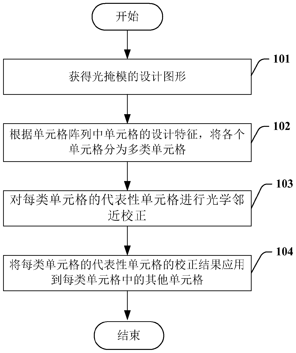
[0025] In order to make the above objects, features and advantages of the present invention more comprehensible, specific implementations of the present invention will be described in detail below in conjunction with the accompanying drawings.

[0026] In the following description, many specific details are set forth in order to fully understand the present invention, but the present invention can also be implemented in other ways than those described here, so the present invention is not limited by the specific embodiments disclosed below.

[0027] As indicated in this application and claims, the terms "a", "an", "an" and / or "the" do not refer to the singular and may include the plural unless the context clearly indicates an exception. Generally speaking, the terms "comprising" and "comprising" only suggest the inclusion of clearly identified steps and elements, and these steps and elements do not constitute an exclusive list, and the method or device may also contain other st...


PUM


Abstract

The invention provides an optical proximity correction method of a photomask. The optical proximity correction method comprises the following steps: acquiring a design pattern of the photomask, the design pattern having a cell array; classifying cells according to the design characteristics of the cells in the cell array; performing optical proximity correction on at least one representative cellof each class of cells; and applying a correction result of the representative cell of each class of cells to other cells of each class of cells.

Description

technical field [0001] The invention mainly relates to the field of semiconductor design and manufacture, in particular to an optical proximity correction of a photomask. Background technique [0002] With the continuous development of the semiconductor manufacturing process, the feature size on the logic device node is close to or smaller than the wavelength used in the photolithography process. According to the principle of light diffraction and interference, light waves will be diffracted when passing through the mask, and the light passing through different positions of the mask will also interfere. Therefore, the light intensity distribution actually projected onto the silicon wafer is the result of the superposition of these diffracted and interfered light waves, which is not exactly the same as the mask pattern. [0003] Optical proximity correction (Optical Proximity Correction, OPC) is the core technology in the nanoscale wafer manufacturing process. With the conti...

Claims


Application Information

Patent Timeline
Patent Type & Authority Applications(China)
IPC IPC(8): G03F1/36
CPCG03F1/36
Inventor 张雷
Owner YANGTZE MEMORY TECH CO LTD
Features
  • R&D
  • Intellectual Property
  • Life Sciences
  • Materials
  • Tech Scout
  • Unparalleled Data Quality
  • Higher Quality Content
  • 60% Fewer Hallucinations
Learn More