Double-sided solar cell and manufacturing method thereof

A technology for solar cells and manufacturing methods, applied in the field of solar cells, capable of solving the problems of large differences in the appearance of PERC double-sided solar cells, low efficiency of the back of the cells, and high reflectivity of the back of silicon wafers, etc., to achieve improved rear efficiency and double-sided ratio , reduce external pollution, beautiful appearance

Active Publication Date: 2020-08-07
CHINT NEW ENERGY TECH (HAINING) CO LTD
View PDF3 Cites 4 Cited by
  • Summary
  • Abstract
  • Description
  • Claims
  • Application Information

AI Technical Summary

Problems solved by technology

[0003] At present, when preparing PERC double-sided solar cells, after the front side of the silicon wafer is diffused to form a pyramid structure, the PSG on the back side is removed by acid etching and the back side is polished, because acid etching is used on the back side. , so that the back reflectivity of the silicon wafer is high, and the light trapping ability is poor, which leads to the low efficiency of the back of the cell. , instead of a pyramid structure, that is, it is different from the type of structure on the front, resulting in a large difference in the appearance of PERC double-sided solar cells

Method used


Image

  • Double-sided solar cell and manufacturing method thereof
  • Double-sided solar cell and manufacturing method thereof

Examples


Embodiment Construction

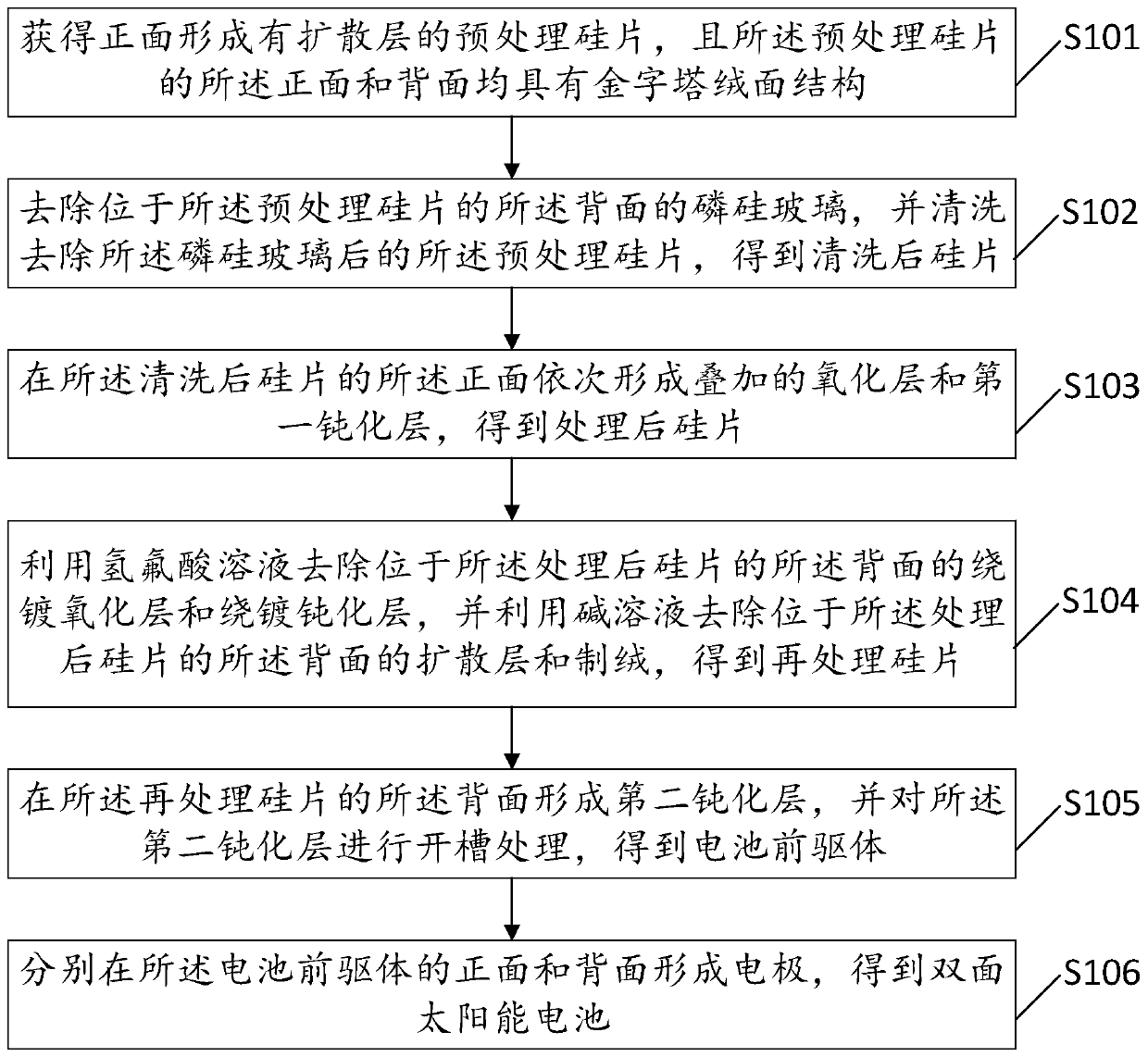
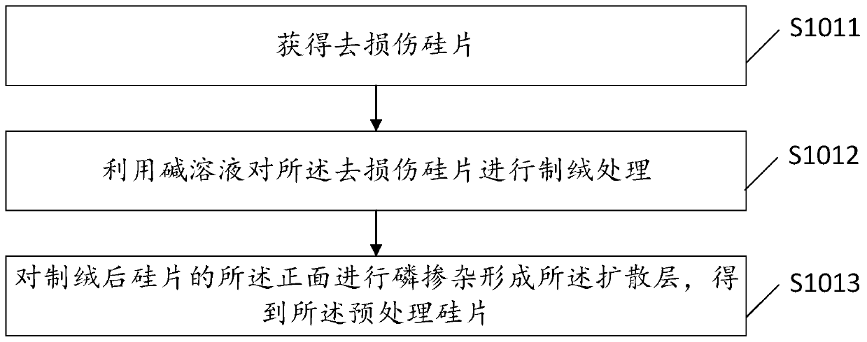
[0036] In order to enable those skilled in the art to better understand the solution of the present application, the present application will be further described in detail below in conjunction with the drawings and specific implementation methods. Apparently, the described embodiments are only some of the embodiments of this application, not all of them. Based on the embodiments in this application, all other embodiments obtained by persons of ordinary skill in the art without making creative efforts belong to the scope of protection of this application.

[0037] In the following description, a lot of specific details are set forth in order to fully understand the present invention, but the present invention can also be implemented in other ways different from those described here, and those skilled in the art can do it without departing from the meaning of the present invention. By analogy, the present invention is therefore not limited to the specific examples disclosed bel...


PUM


Abstract

The invention discloses a method for manufacturing a double-sided solar cell, and the method comprises the steps: obtaining a preprocessing silicon wafer with a diffusion layer formed on the front surface, and enabling the front surface and back surface of the preprocessing silicon wafer to have pyramid suede structures; removing phosphorosilicate glass on the back surface of the preprocessing silicon wafer, and cleaning the preprocessing silicon wafer from which the phosphorosilicate glass is removed to obtain a cleaned silicon wafer; sequentially forming an oxide layer and a first passivation layer which are superposed on the front surface of the cleaned silicon wafer to obtain a treated silicon wafer; removing the winding plating oxide layer and the winding plating passivation layer onthe back surface of the treated silicon wafer by using a hydrofluoric acid solution, and removing the diffusion layer and texturing on the back surface of the treated silicon wafer by using an alkaline solution to obtain a retreated silicon wafer; forming a second passivation layer on the back surface of the retreated silicon wafer, and slotting the second passivation layer to obtain a battery precursor; forming electrodes on a front surface and a back surface of the battery precursor to obtain the double-sided solar cell, thereby effectively improving the double-sided rate of the cell and reducing the color difference between the front surface and the back surface.

Description

technical field [0001] The present application relates to the technical field of solar cells, in particular to a double-sided solar cell and a manufacturing method thereof. Background technique [0002] PERC (passivated emitter and rear contact, passivated emitter and rear contact) battery has become a research hotspot in the photovoltaic industry because of its good back passivation structure, which can improve the opening voltage and short-circuit current of the battery. [0003] At present, when preparing PERC double-sided solar cells, after the front side of the silicon wafer is diffused to form a pyramid structure, the PSG on the back side is removed by acid etching and the back side is polished, because acid etching is used on the back side. , so that the back reflectivity of the silicon wafer is high, and the light trapping ability is poor, which leads to the low efficiency of the back of the battery. , instead of a pyramid structure, that is, it is different from th...

Claims


Application Information

Patent Timeline
Patent Type & Authority Applications(China)
IPC IPC(8): H01L31/18H01L31/0236H01L31/068
CPCH01L31/1804H01L31/0684H01L31/02363Y02E10/547Y02P70/50
Inventor 廖晖马玉超单伟何胜徐伟智
Owner CHINT NEW ENERGY TECH (HAINING) CO LTD
Why Eureka
Try Eureka