Compensation for substrate doping for in-situ electromagnetic inductive monitoring

An electromagnetic induction and substrate technology, applied in the direction of using electromagnetic means, using electrical devices, grinding machine parts, etc., can solve problems such as non-uniformity, reduce non-uniformity, improve reliability, and avoid insufficient grinding.

Pending Publication Date: 2020-08-07
APPLIED MATERIALS INC
View PDF10 Cites 1 Cited by
  • Summary
  • Abstract
  • Description
  • Claims
  • Application Information

AI Technical Summary

Problems solved by technology

Thus, determining the grinding endpoint with respect to grinding time alone may result in non-uniformity within the wafer or from wafer to wafer

Method used


Image

  • Compensation for substrate doping for in-situ electromagnetic inductive monitoring
  • Compensation for substrate doping for in-situ electromagnetic inductive monitoring
  • Compensation for substrate doping for in-situ electromagnetic inductive monitoring

Examples


Embodiment Construction

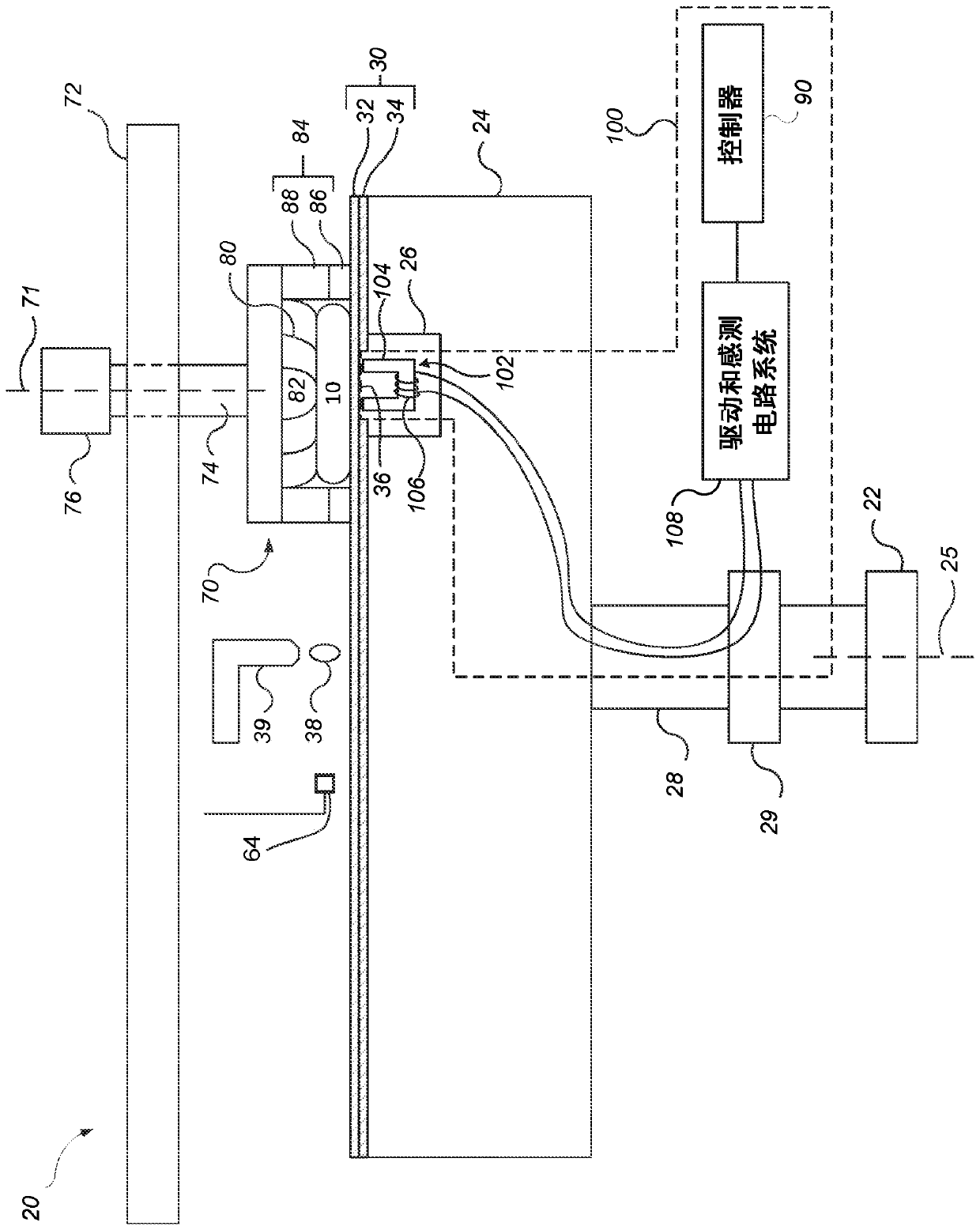
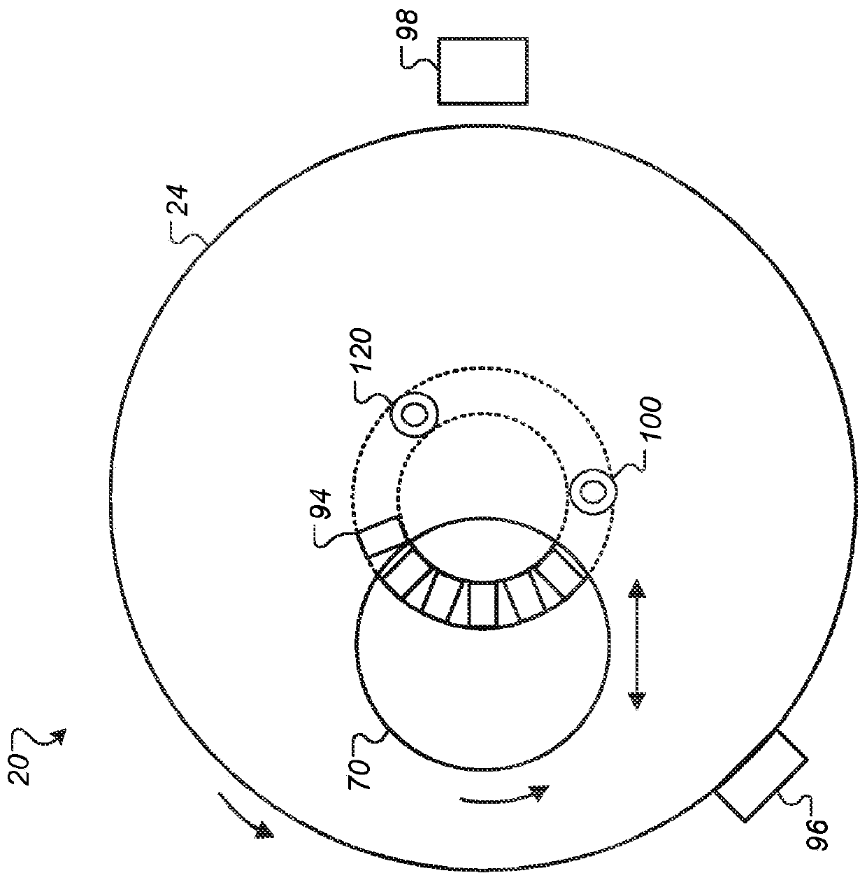
[0020] One monitoring technique for grinding operations is to induce eddy currents (eg, using an alternating current (AC) drive signal) in a conductive layer on the substrate. Induced eddy currents can be measured in situ by eddy current sensors during grinding to generate a signal. Assuming that the outermost layer undergoing grinding is the conductive layer, the signal from the sensor should depend on the thickness of the conductive layer. Based on the monitoring, control parameters of the milling operation (eg, milling rate) can be adjusted in situ. Additionally, the milling operation may be terminated based on an indication that the monitored thickness has reached a desired endpoint thickness.

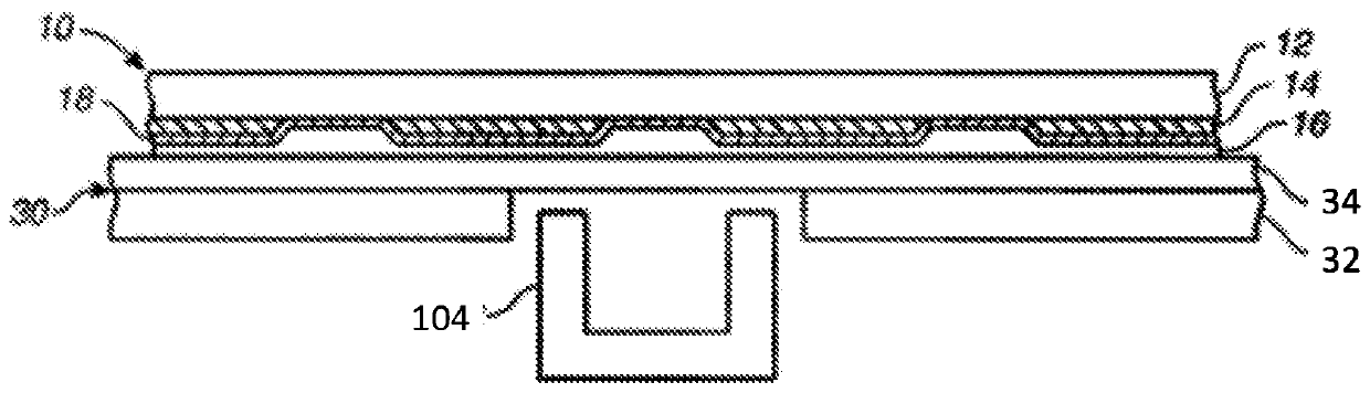
[0021] In fact, the magnetic field generated by an eddy current sensor does not stop within the conductive layer, but can extend into the underlying substrate. Without being bound by any particular theory, the skin surface depth in these magnetically permeable materials for the e...


PUM


Abstract

A method of chemical mechanical polishing includes bringing a substrate having a conductive layer disposed over a semiconductor wafer into contact with a polishing pad, generating relative motion between the substrate and the polishing pad, monitoring the substrate with an in-situ electromagnetic induction monitoring system as the conductive layer is polished to generate a sequence of signal values that depend on a thickness of the conductive layer, determining a sequence of thickness values for the conductive layer based on the sequence of signal values, and at least partially compensating for a contribution of conductivity of the semiconductor wafer to the signal values.

Description

technical field [0001] The present disclosure relates to chemical mechanical polishing, and more particularly to monitoring conductive layers during chemical mechanical polishing. Background technique [0002] Integrated circuits are typically formed on a substrate by sequentially depositing conductive, semiconductive, or insulating layers on a silicon wafer. Various fabrication processes require planarization of layers on a substrate. For example, one fabrication step involves depositing a fill layer on a non-planar surface and planarizing the fill layer. For some applications, the fill layer is planarized until the upper surface of the patterned layer is revealed. For example, a metal layer may be deposited on a patterned insulating layer to fill trenches and holes in the insulating layer. After planarization, the remainder of the metal in the trenches and holes of the patterned layer forms vias, plugs, and lines to provide conductive paths between thin film circuits on...

Claims


Application Information

Patent Timeline
Patent Type & Authority Applications(China)
IPC IPC(8): B24B49/10B24B7/22
CPCB24B37/005B24B37/27B24B49/105G01B7/105B24B7/228G01B7/10
Inventor 鲁伟D·M·盖奇H·Q·李K·徐J·张
Owner APPLIED MATERIALS INC
Why Eureka
Try Eureka